

Pocket Computer Universal Interface
Features Summary
- Provides cassette interface emulation to read and write programs and data directly to and from a micro SD card.
- Provides a printer interface between the pocket computer or calculator and most standard “line printers” such as dot matrix, thermal receipt printers, serial, parallel, and Wi-Fi.
- Supports printing of custom glyphs, including math, scientific and engineering symbols unique to each model.
- Works independently without a computer and can be powered by a single 18650 lithium ion rechargeable battery.
- OLED screen with user-friendly menu system and operating modes
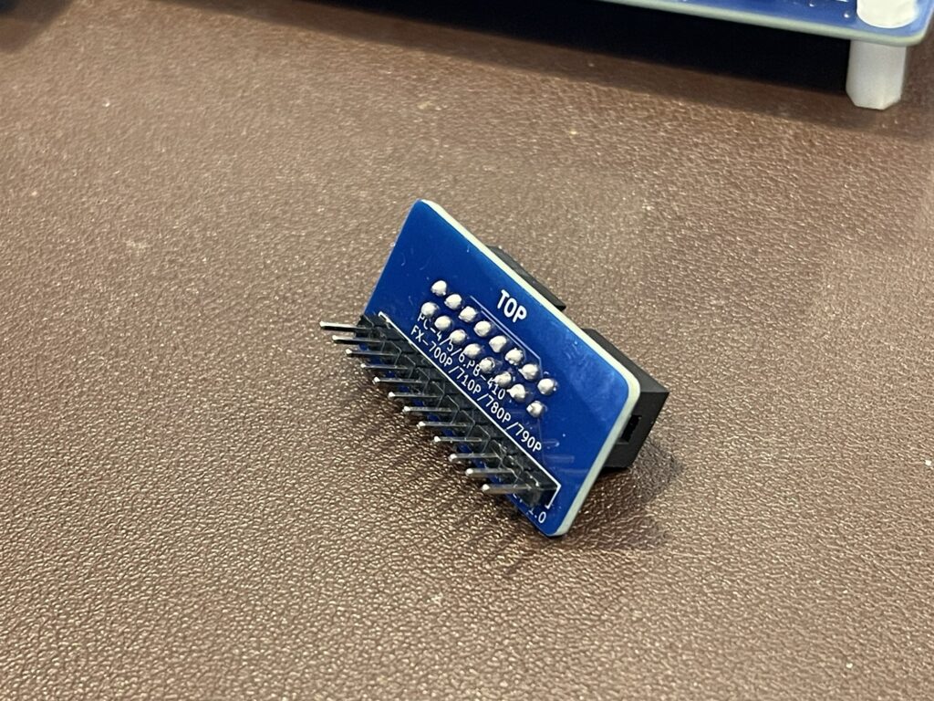
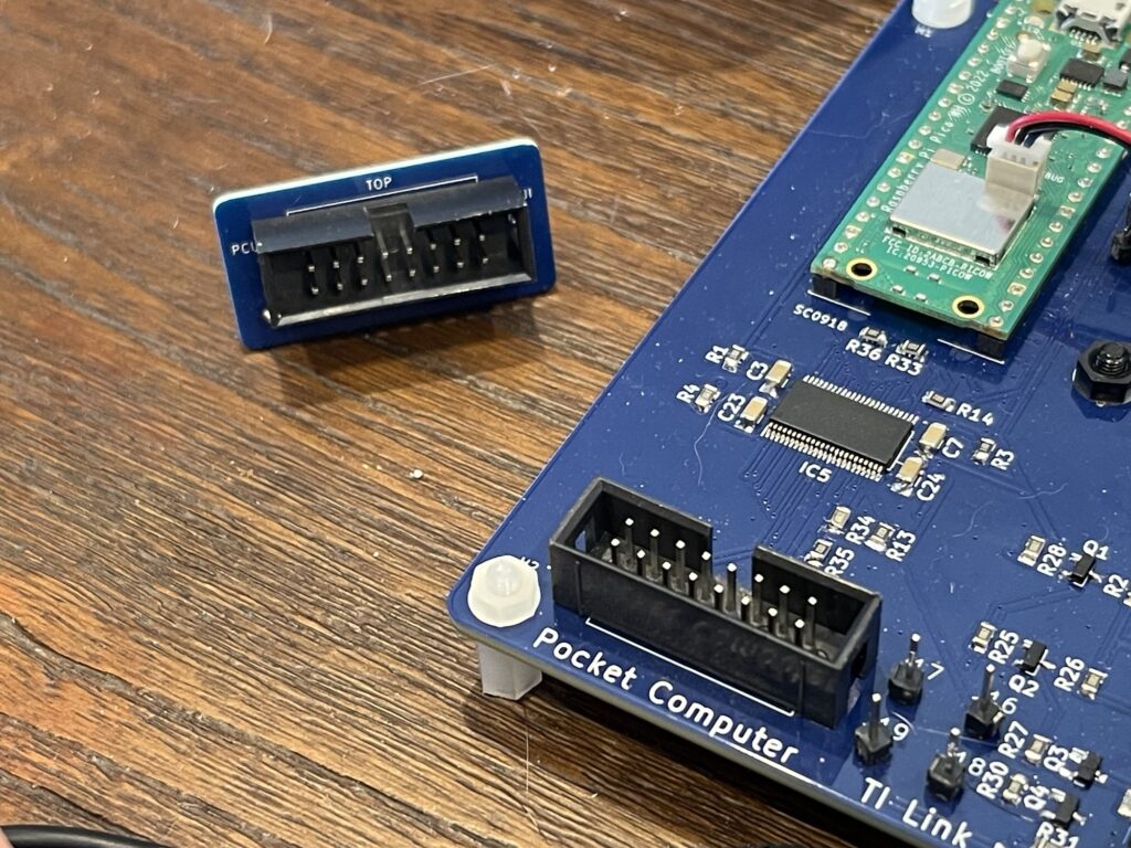
- Interface packs provide connectivity to each supported model, no need for OEM connection cables.
- Updatable firmware and PC or Mac connectivity via USB for mounting micro SD card
- Plotter emulation mode to provide printouts of plots using modern printers allowing programs which leveraged plotter features to be used on modern printers.
- ASCII BASIC conversion to and from tokenized BASIC “on the fly”, allowing for program edits and program creation on a Mac or PC and directly sending it to a pocket computer.
- Wi-Fi connectivity and web interface for program viewing, editing, UI control, printing, and status.
- True low-level cassette interface integration – byte level retrieval and storage of programs and data images, not just a simple “record” and “playback” mechanism.
Supported Models
The following models are currently supported with more models in progress:
| Brand | Model(s) |
| Texas Instruments | Graph Link Graphing Calculators TI-82*, TI-85*, TI-86*, TI-89*, TI-92*, TI-92 Plus*, Voyage 200* |
| Sharp Radio Shack | 9-Pin “CE-121” / “CE-122” Compatibles PC-1210, PC-1211, PC-1212, TRS-80 PC-1* |
| Sharp Tandy | Older 11-pin “CE-126P” Compatibles PC-1245, PC-1246, PC-1246S, PC-1247, PC-1248, Tandy PC-8* PC-1250, PC-1250A, PC-1251, PC-1251H, PC-1255, Tandy PC-3* and PC-3 A/B*, PC-1270 |
| Sharp | Newer 11-pin “CE-126P” Compatibles PC-1401, PC-1403*, PC-1421, PC-1430, PC-1450, EL-5500, EL-5500 II, EL-5500III* |
| Casio Radio Shack Tandy | 12-pin PB-100 Series, FP-12(S) Compatibles PB-100, PB-110, PB-120, PB-200, PB-400, PB-410*, FX-700P, FX-710P, Tandy PC-4 Version B*, TRS-80 PC-4 Version A* |
| Casio Tandy | 12-pin FX “Clamshell” Series FX-770P, FX-780P, FX-781P, FX-785P, FX-790P, FX-791P, FX-795P, Tandy PC-5*, Tandy PC-6* |
| Casio | 15-pin FA-10 / FA-11 Compatibles PB-700*, PB-770* |
| Casio | FX-702P*, FX-602P* |
The firmware, documentation, and related files are located on the PCUI Github page.
Background
I have been experimenting with several pocket computers over the years. The brands of these pocket computers are usually either Sharp or Casio. The Radio Shack models are either rebranded Sharp or Casio models as well.
Whether it be a Sharp or Casio device, each has their proprietary peripherals, such as printers, cassette interfaces, and serial ports. Very few have peripherals with parallel ports, which is convenient for using standard line printers.
As time goes on, it becomes more and more difficult to find these obscure and vintage printers, cassette interfaces and interface boxes. Several hobbyists have created their own interfaces for connection to PCs for example, and many are decades old by now.
As I have experimented with various models of pocket computers, each has their own printer, for example, and each usually has some obscure quirk rendering them almost obsolete these days.
For example, one particular printer I have needs aluminum coated paper which is all but unobtainable these days. Others use tiny plotter pens, also unobtainable these days. Fortunately there were some pocket computer printers which were thermal and had used paper that is still available today. Even so, these are not easy to find these days.
The early pocket computers would have interface ports that were simply it’s bus exposed for printers and cassette interfaces to be able to read the bus. Later models would include more familiar parallel and serial pins, which can easily be connected to RS-232 drivers and buffers for example. The earlier pocket computers are the most challenging to build an interface for, as these expansion ports were not simple serial or parallel connections.
A New Project – Vision and Scope
In the age of inexpensive microcontrollers, I wanted to experiment to see if I could use one of these microcontrollers to interface with a pocket computer.
Ideally, it would be useful to have a single device that can be connected to various Sharp and Casio models and software configurable as to which device it is connected to.
The device would then emulate the pocket computer’s respective printer and cassette interface for example.
The device would plug into the pocket computer and effectively be a bridge to a standard parallel or serial printer and perhaps a MicroSD card as a cassette storage emulator. This would allow anyone with only the pocket computer and this device to be able to print to a printer and save and load programs.
The benefit of this device would be twofold. One, it would allow for those who may have only the pocket computer and none of the peripherals to be able to save and load programs as well as print. Finding the respective printers and cassette interfaces these days is difficult and can be expensive.
Second, this device could be built quite inexpensively by those who might have some basic electronics skills, or, purchased pre-assembled, again, at a lower price compared to sourcing the original peripherals on auction sites.
The device could eventually be compatible with several models of both Casio and Sharp Pocket computers as well as others.
The device itself would be simple, using a microcontroller with onboard flash to store the firmware, a serial port and a parallel port. Power for the device would need to be provided, either by a battery or USB connection for example.
Computers these days do not necessarily have RS-232 ports, and USB based serial ports are common. This device can have a USB port with a serial port embedded providing both a serial port for a PC connection for additional integrations and it could also be an optional power source for the device itself.
For the first round of features, I will not be focusing on the bigger expansion bus found on some models, such as the Casio PB-1000, Sharp PC-1500, or the FX-880P. I will instead focus only on the simpler interface pinouts, such as the Casio PB-100 series and the Sharp PC-1211 for example.
The printer I plan to use is an inexpensive Epson POS thermal receipt printer. These printers are fast, use inexpensive paper and are easy to obtain.
Inexpensive Microcontrollers
There are several microcontroller platforms to choose from, including the Pico, ESP32, Arduino, and others. All of these options are far less expensive and capable these days compared to 25 years ago as an example.
My last experience with microcontrollers was with a Motorola 68HC12 and programming in assembly. The project was a digital answering machine using a series of ISD voice recorder ICs, an audio multiplexer, an LCD display and some buttons.
At the time, this was the late 90s, and a development kit for the HC12 was well over $300. A debug tool would then cost a few hundred dollars more. On a college budget, this was expensive.
Not to mention the flash on the HC12 was rated for only about 100 erase cycles. This meant that I was bound to loading my program in its RAM for development, and flash only working subroutines.
After watching a series of videos released by Cornell University on the Raspberry Pi Pico, and being familiar with the Raspberry Pi in general, I decided to look into a design centered around a Pico 2.
These days, a Raspberry Pi Pico 2 board is around $8 each, mounted to a typical DIP style package.
This package at $8 is similar to my HC12 kit back then. It has all of the supporting components needed on the PCB such as a clock, reset, bootloader, debug connector, and a power supply circuit.
Since it is now much later than the 90s, USB, Wi-Fi and Bluetooth are ubiquitous these days. Many of these types of microcontrollers have these onboard.
There is plenty of onboard flash and RAM, and no worry of wearing out the flash erase cycles (it is now rated at hundreds of thousands of cycles).
Reverse Engineering
Plenty of hobbyists have built their own interfaces for these pocket computers, and some have provided documentation on the circuits and software. I have found quite a bit of documentation on the PB-100 series bus interfacing, and quite a bit on the Texas Instruments TI-85, 86, 92, and other graphing calculators from the 1990s.
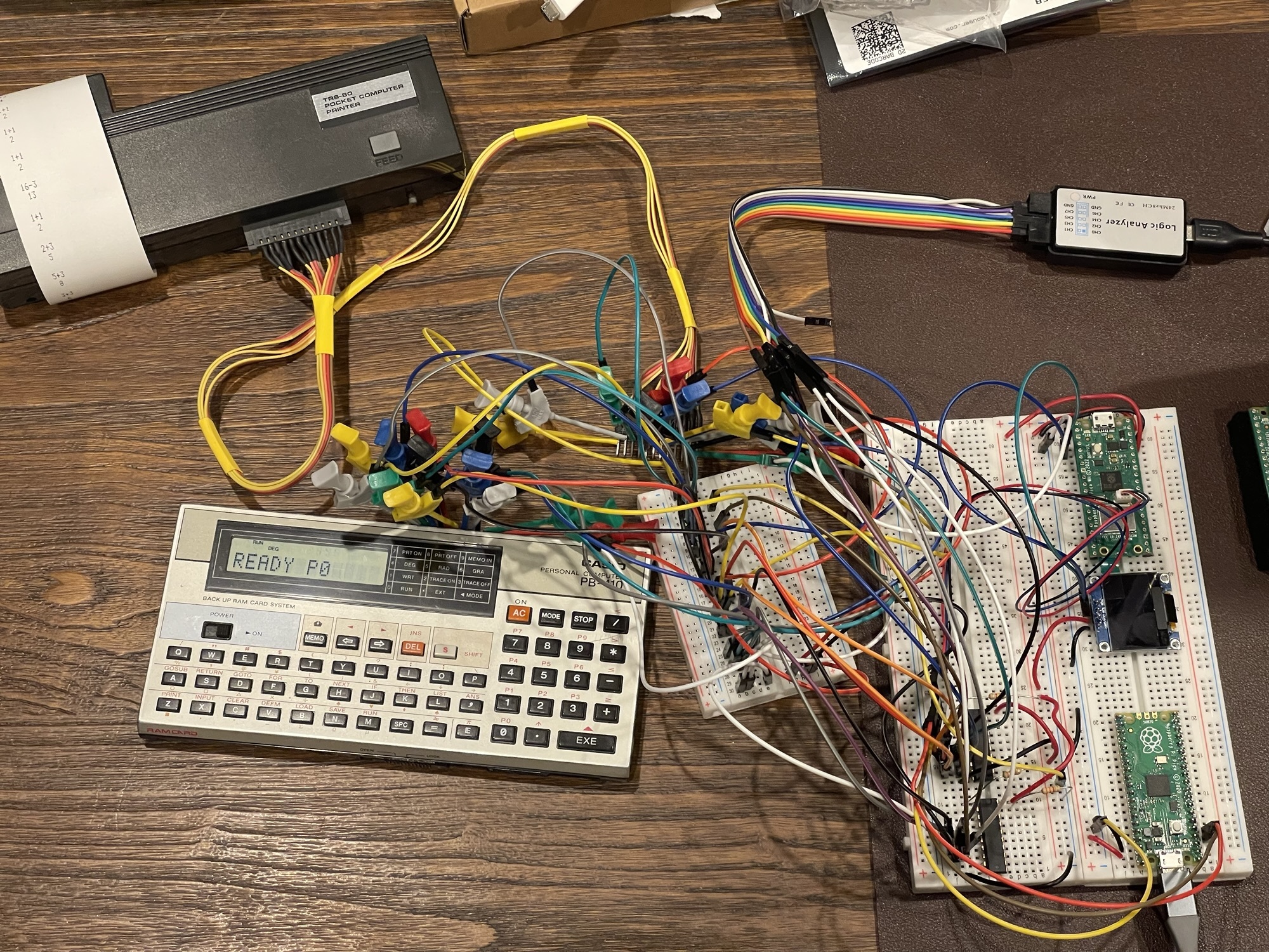
For the other models, I can reverse engineer the bus interfaces using the peripherals I own and a logic analyzer for example.
I could combine documentation which others have provided, the service manual for the expansion port pinout, a scope, and logic analyzer for discovering the interface protocol.
As an example, I started with the Tandy PC-6 pocket computer. It uses a 12-pin peripheral port, and is compatible or the same as the PC-4 and PC-5. It is also compatible with the Casio PB-100 series (including the PB-410 for example) and the FX-780 and FX-790 as well as many others.
The printer for these was the FP-12S which is quite a small thermal printer and not too commonly found these days.
The FP-40 is a bigger thermal printer, but the interface packs needed to connect it to these models is rarely available anywhere these days.
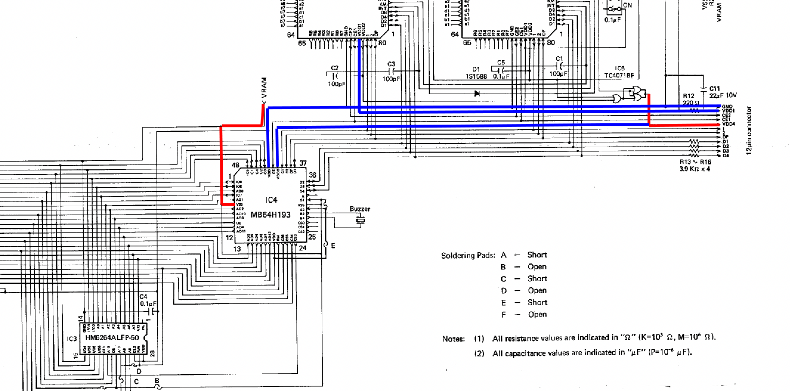
PC-6 Architecture
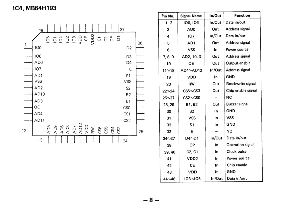
To provide an example of the type of interfacing used in these pocket computers, the PC-6 can be inspected and used as a reference. The PC-6 uses two 4-bit CPUs which share control of the display and keyboards (upper and lower), and a gate array (IC4) provides the interface to the RAM:
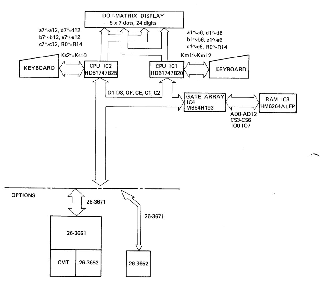
Notice the RAM does not have any address lines from the CPU. Only 4 data lines, CE, OP are used to address, read, and write to the RAM. The gate array must control the addressing, reading and writing to and from the RAM.
The PC-6 service manual includes the pinout for the 12-pin peripheral port:
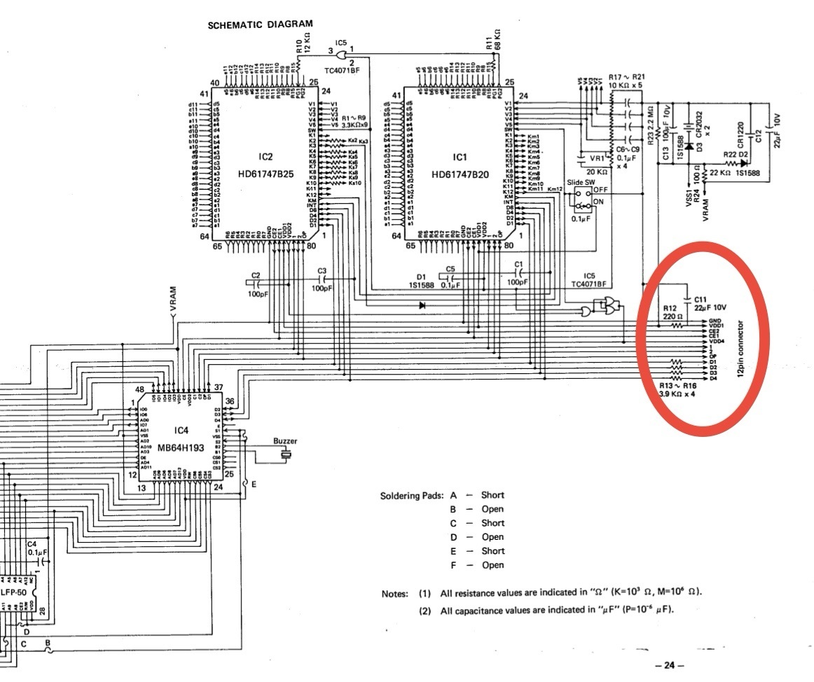
The peripheral data bus is also 4-bit and has two voltages present (VDD1 and VDD4), two chip enable pins (CE1 and CE2) and 3 other pins, 1, 2, and OP.
The pins D1 through D4 are the 4-bit data bus, as those are connected to IC4 and the two processors, IC1 and IC2. IC4 interfaces the memory to the bus and is controlled via opcodes. Since several devices are connected to the data bus, each device must support three states: input, output, and high impedance. If I am to attach anything to these pins, it must also support these three states, defaulting to a high impedance state (appearing as if it is disconnected from the circuit).
Pins 1 and 2 are clock signals, since they are inputs to C1 and C2 on IC4.
OP is an input to the IC4 gate array, but is both an input and output for both CPUs (IC1 and IC2). Since my circuit will need to control IC4, my interface will need to be an input and an output.
VDD1 is connected to the power switch, while VDD4 is a signal indicating the power state of the system, i.e. “on” or in an auto power off state.
Observation
In order to observe what the PC-6 expansion port pins are doing when connected to a printer or cassette interface, I would need to connect the PC-6 to its printer and then probe each line.
I connected the PC-6 expansion port to a breadboard, then the printer to the breadboard. This provides for points to connect a scope, logic analyzer, and the Pi Pico.
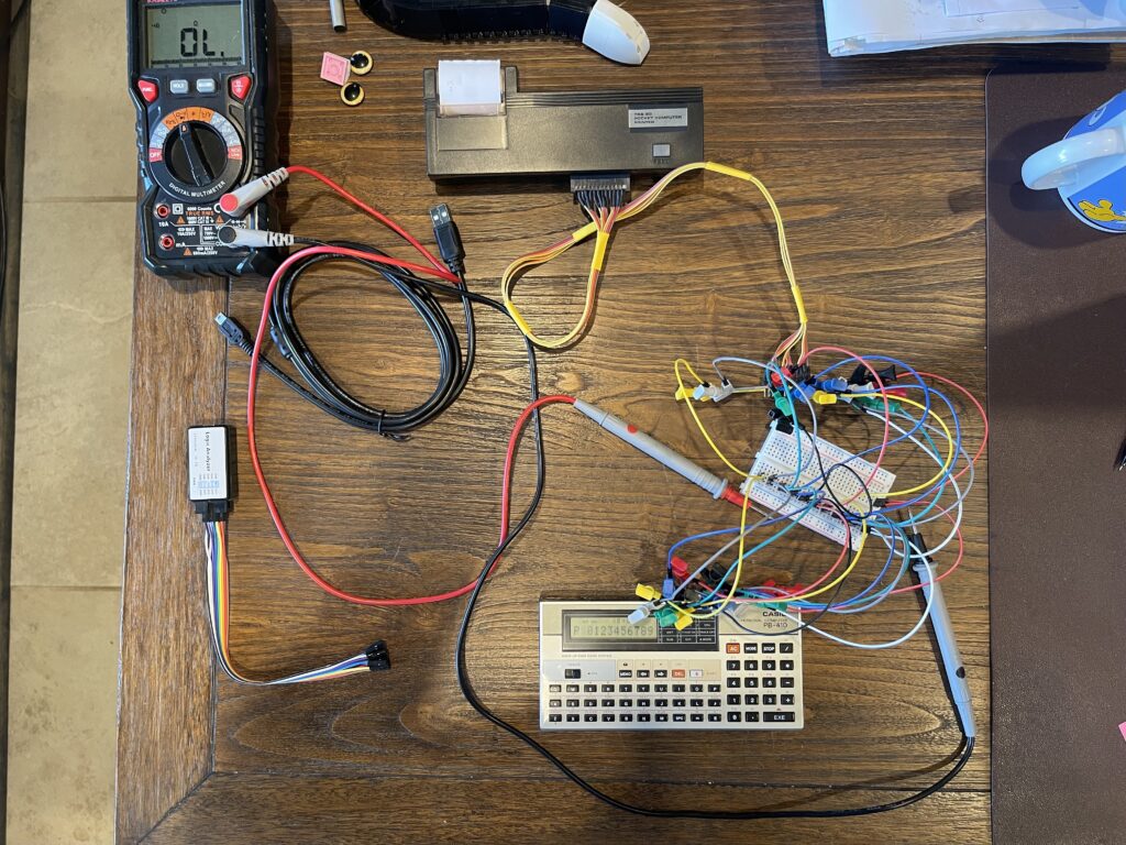
First, I would be curious what level VDD1 and VDD4 are at. Before going any further, I checked the voltage levels on the PC-6, specifically VDD1 and VDD4 compared to the GND pin on the port. The Pi Pico uses CMOS logic levels, that is levels of 0V and 3.3V. This is not the same as TTL logic levels of 0V and 5V. There are buffer ICs that can handle the voltage translation between these two types of interfaces.
I needed to determine if the PC-6 was using CMOS or TTL logic levels.
When using the GND pin as a reference, VDD1 was -5V and VDD4 was -5V. VDD4 is not present when auto power off occurs. This means the voltage at VDD4 will be present only when the computer is on. Further, all of the other signals were 0V or -5V, not what I initially expected. I measured this with a scope.
If I use the GND pin as a ground reference, the logic signals on the bus will be 0V and -5V, which is not within range of what the Pi Pico will handle. I would have expected levels between 0V and 5V.
Solution to the Negative Logic Levels
After quite a bit of thinking, looking over the schematic in the service manual, more thinking, I figured out that if I use VDD1 as a ground reference, all of the logic lines on the bus then fall into the range I expect, 5V or 0V.
Now that I had the logic levels sorted out, the next step was to take a peek at the bus when the computer is printing.
Logic Analyzer
Since I do not have access to lab-grade equipment and to make it a bit easier to visualize, I used an inexpensive USB logic analyzer, which has 8 ports. These cost around $12 USD.
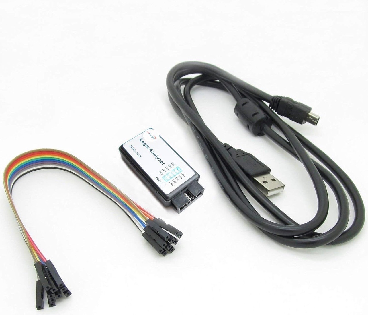
I can look at up to 8 lines at once with this device, which is a bit easier than using a scope for looking at more than 2 or 4 lines at once. I connected the logic analyzer to the bus, specifically pins CE2, CE1, CLOCK 1, CLOCK 2, OP, D1-D3 as a start. I then printed something to the printer while running a capture:
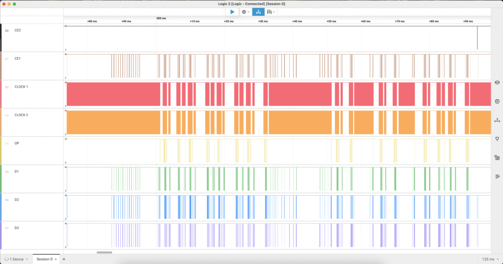
This along with the documentation others have provided on this particular bus interface was quite helpful in developing a hardware and software solution to interface with pocket computers using a tri-state TTL bus.
Texas Instruments Graphing Calculators
The Texas Instruments graphing calculators from the 90s and early 2000s used a 3-wire serial interface to link two calculators together, and to link up to a PC. The calculators included a graph link cable in the box, and the PC link kit could be purchased separately.
These PC link connection kits were a bit expensive, as I had one myself. I used it for transferring programs and screen captures which could be printed.
These days, these interface kits can be found on auction sites, or they can be built. Most these days use USB connections. There is even a library, TILP, a platform for interfacing to these graphing calculators. This library works very well and can use the TI graph link cables.
The link interface uses 5 volt TTL levels. One pin is ground, the two other pins are used for sending and acknowledging. The sender will pull one line low (the line pulled low indicates either a zero or one, depending on which line is pulled low), and the receiver will pull the other line low to acknowledge. The sender raises their line, the receiver raises their line, and the process repeats.
This type of serial connection works without a specified baud rate. It works as fast as the interface itself can support and the processing speed on both ends. Since each bit is acknowledged, it is fairly reliable and robust.
Adding support for this to the pocket computer universal interface would be straightforward. All that would be needed is a 2 wire TTL interface similar to I2C or SPI.
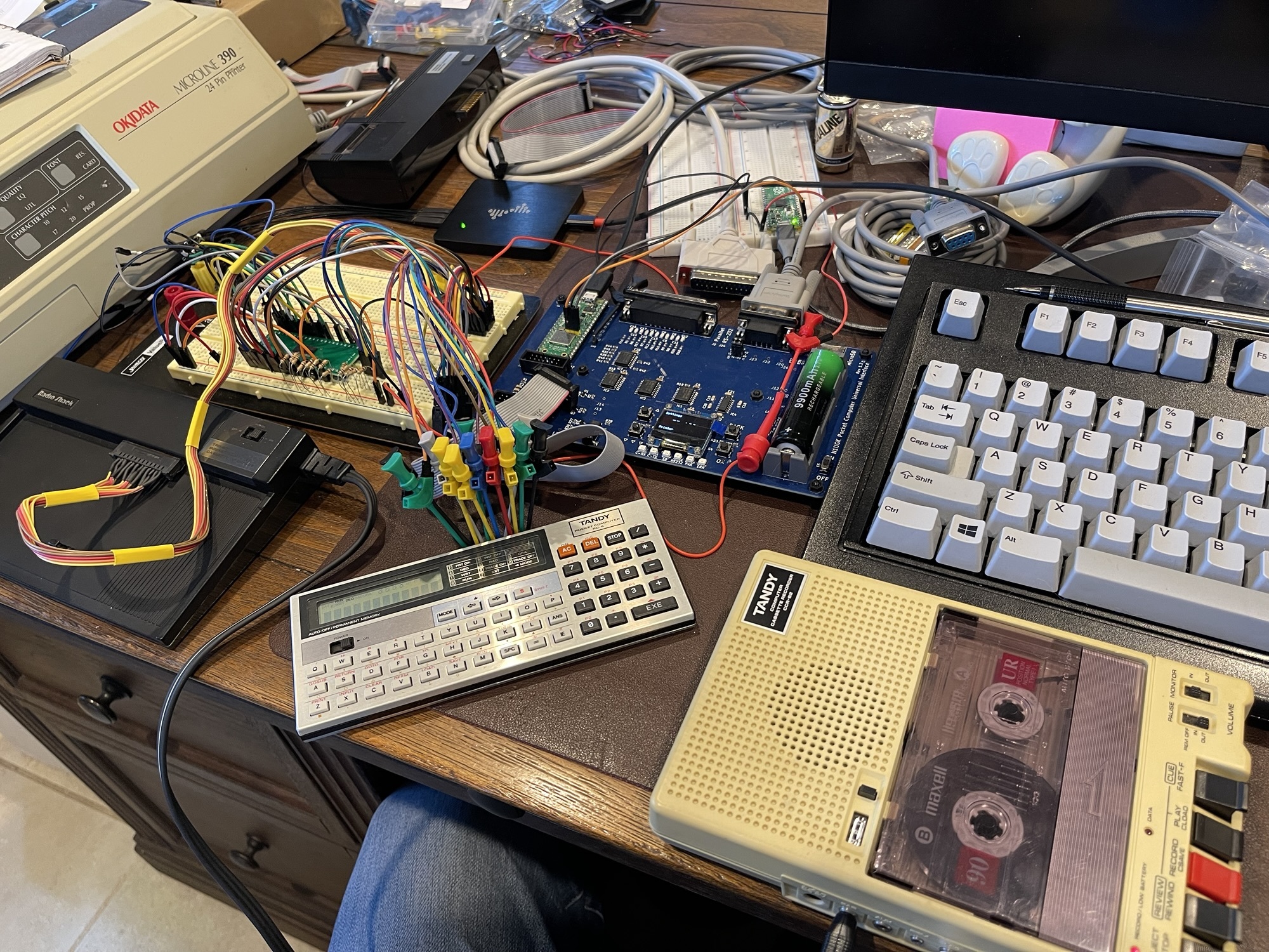
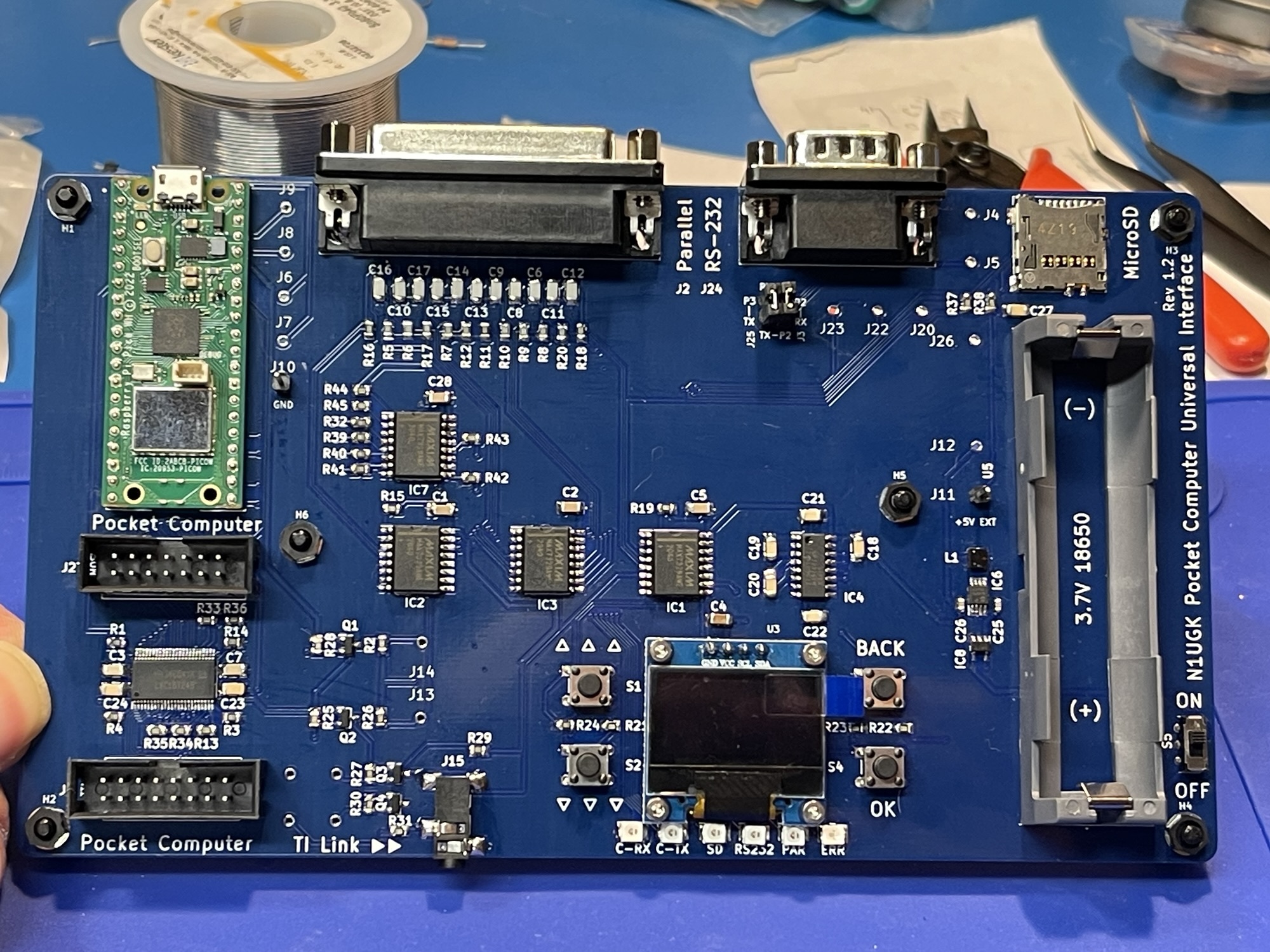
PCUI Hardware Design
Based on the examples described above, the PCUI will need to interface with 5 volt TTL level logic. It will need to support open drain or open collector style interfacing as well as tri-state bus interfacing.
Since the Pico uses CMOS or 3.3 volt logic, voltage level shifting will be required. Since the Pico can be powered by USB and it has a built-in power supply, it can drive both it’s own power needs at 3.3 volts, and other 5 volt devices can be powered from the USB bus supply.
However, since the PCUI might be used in a portable environment, or without a USB host, it would benefit from having its own power source, such as a rechargeable lithium ion battery. This battery could be charged from the USB port.
Since most components these days are surface mount, fewer and fewer components are available in through-hole versions. This means breadboarding or simple home-made PCBs are not practical.
Inexpensive Hobbyist PCB Prototyping
There are several PCB manufacturers that can make prototype boards inexpensively. Technology and automation have made this a reality for those who need to manufacture very few boards, such as less than 100 boards as an example. This was not the case years ago.
This type of readily available on-demand manufacturing allows hobbyists to design a PCB layout and send off the design for manufacture.
The PCB design is performed using EDA software such as KiCad, an open source platform. KiCad can be used to create a schematic of a circuit or layout, and then a PCB designer feature is utilized to layout the components and traces on a PCB.
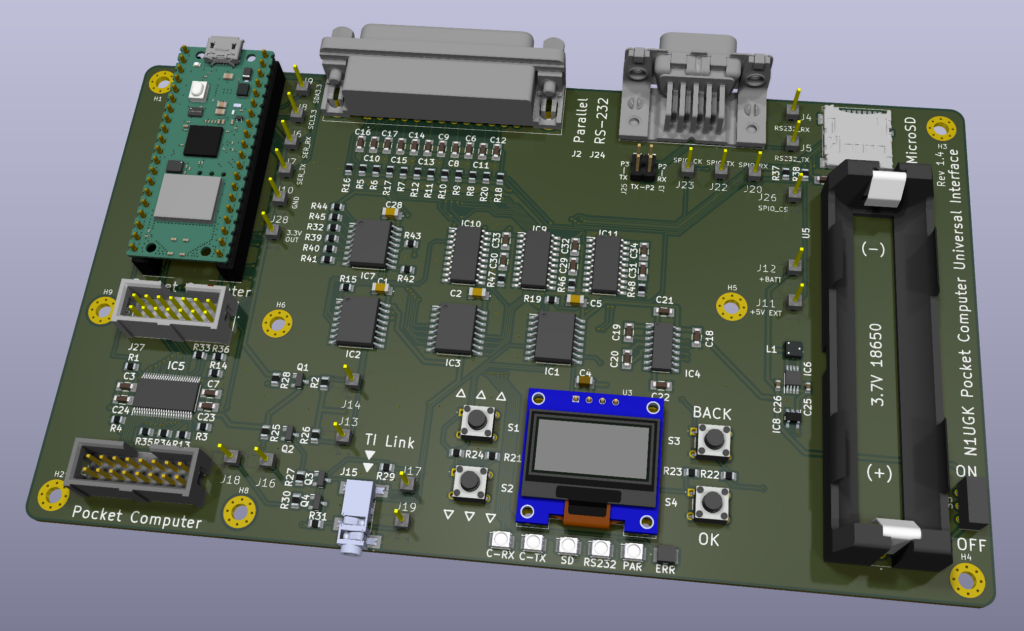
The image above is from the 3D viewer inside the KiCad PCB designer. The components are models which can be downloaded and copied to a library in KiCad. This allows the designer to actually see the layout with pad and footprint clearances before actually manufacturing anything.
Prototyping and Testing
Once the layout is completed, fabrication files can be exported from KiCad and sent off for manufacturing of the PCB. Some manufacturers can also place the components as well, although this costs more.
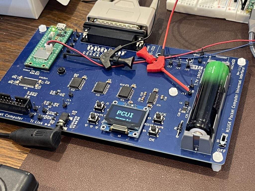
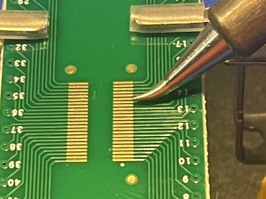
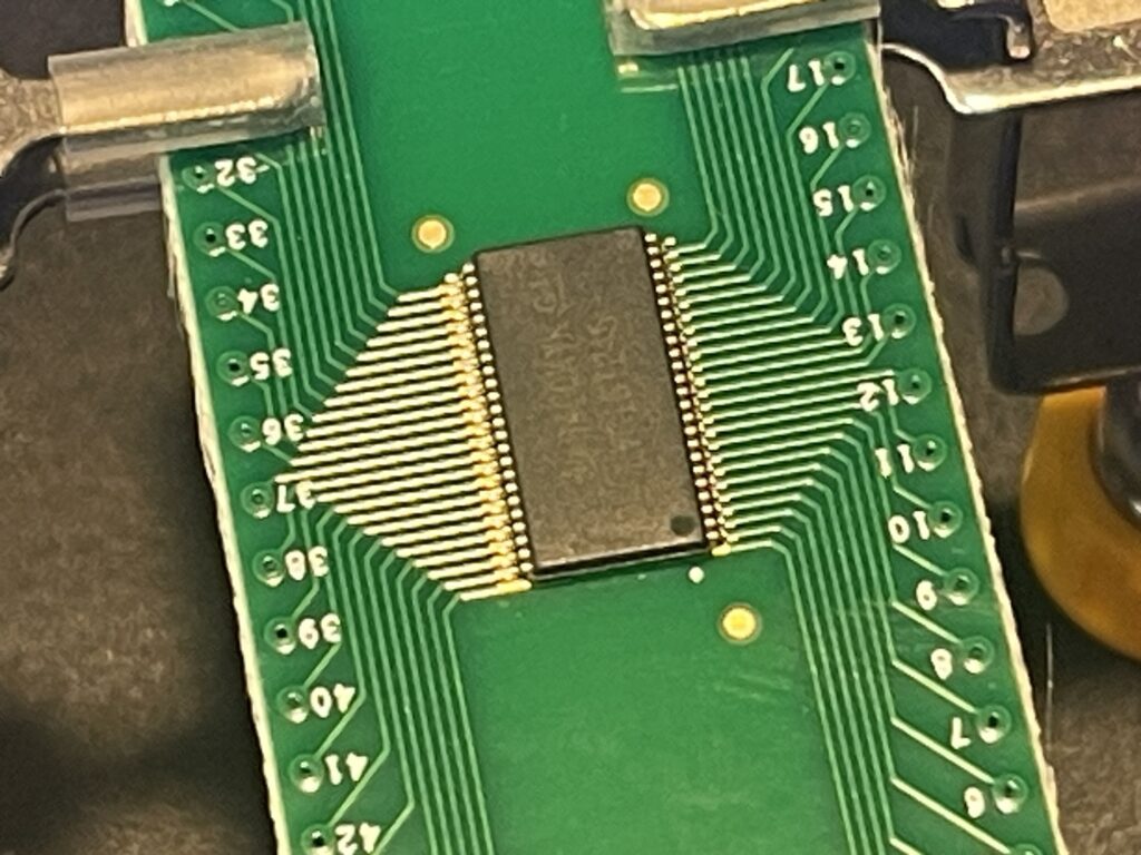
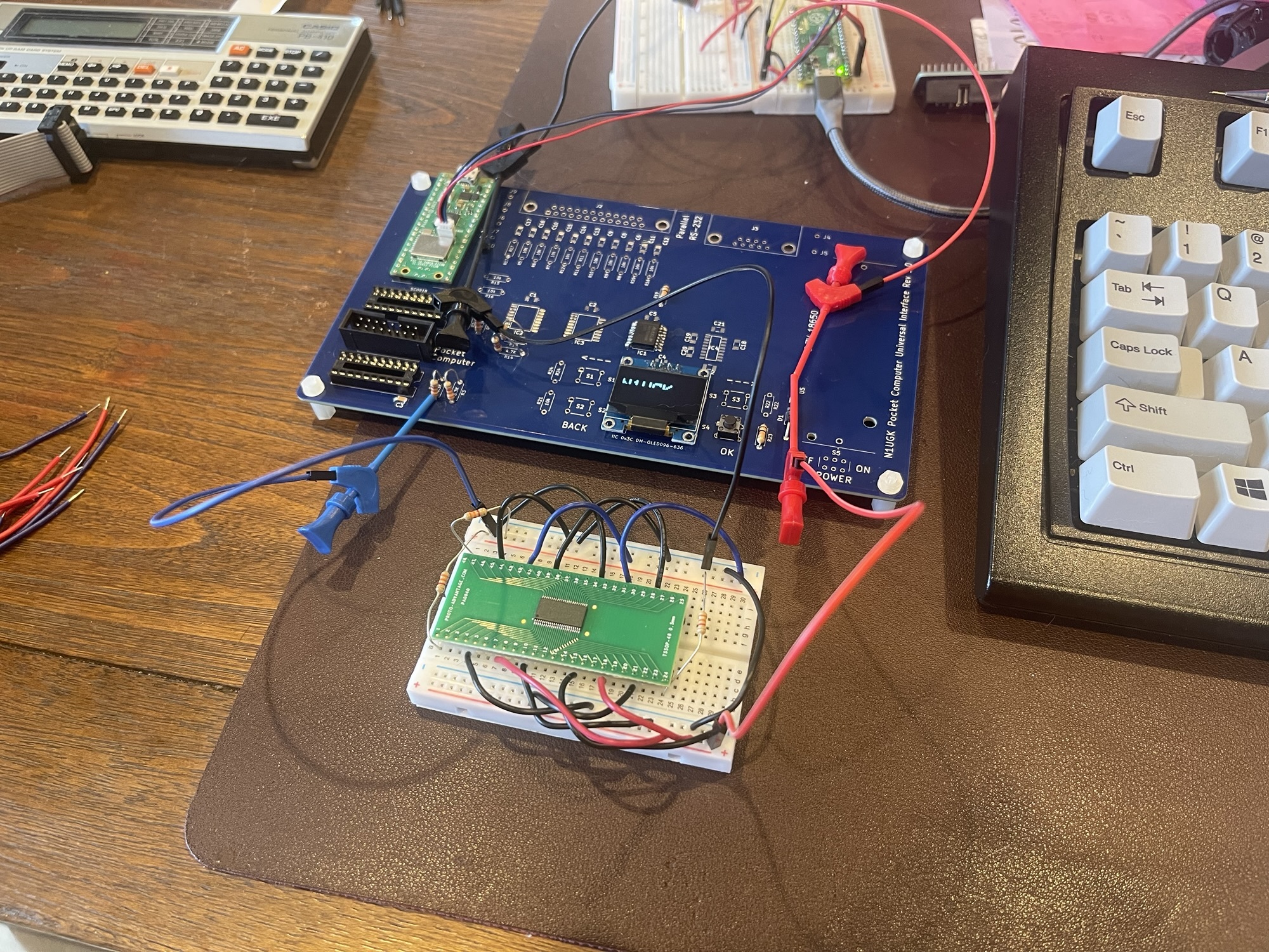
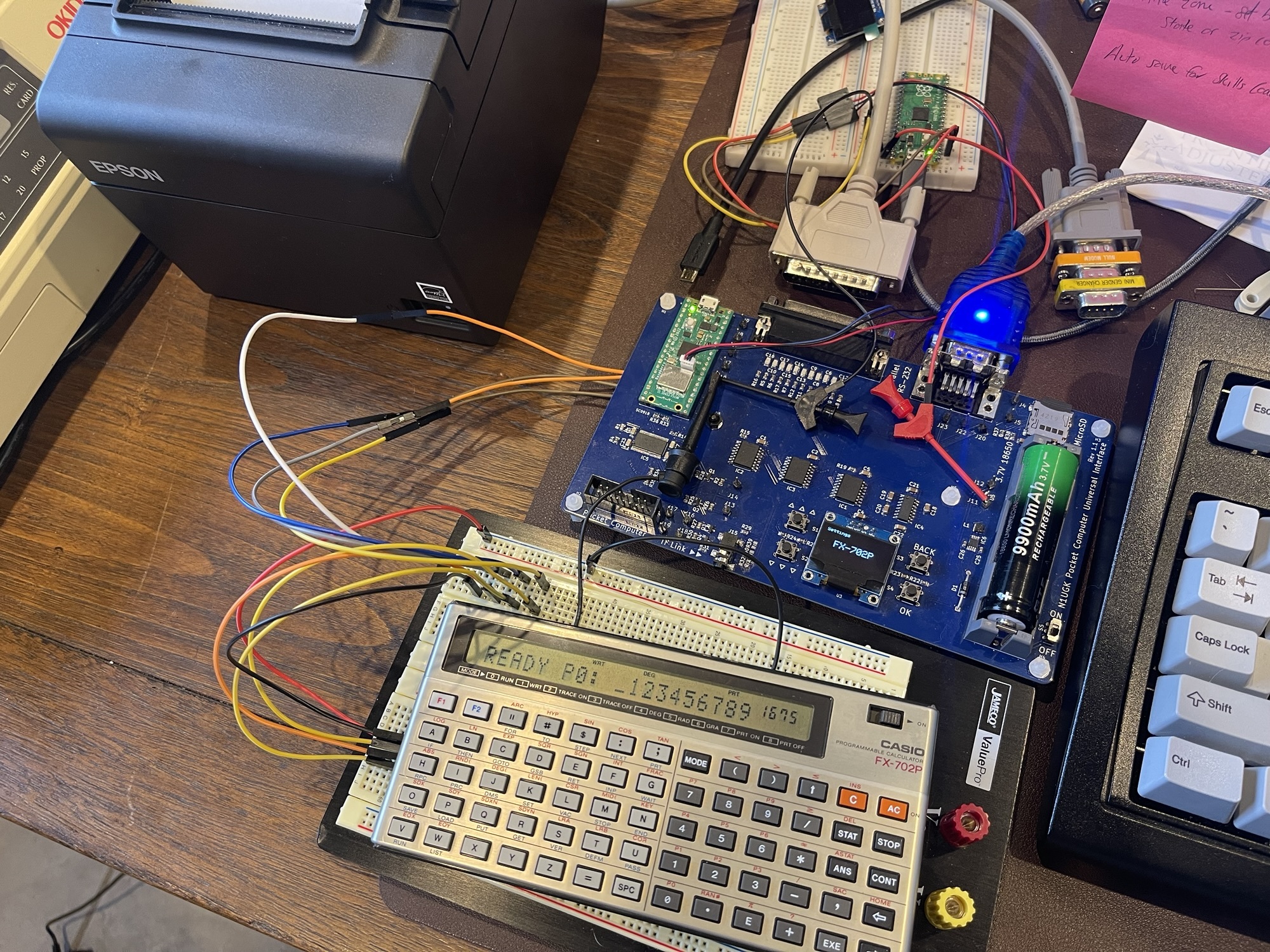
The PCUI has a main PCB with all of the components needed for interfacing between pocket computers, printers, PCs, and more.
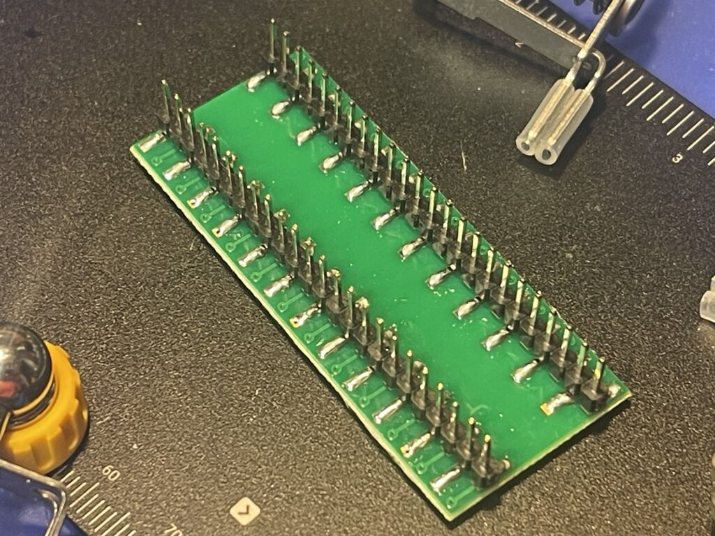
For pocket computers, many have different styles of connectors, all proprietary. The concept with the PCUI is to be able to use the same device for interfacing, with one software platform, but have different connectors for each pocket computer. Each connector or “interface pack” will have its own trace layout for interfacing with the PCUI main board. A standard ribbon cable style connector is used for each variation.

For the PCUI project, I ordered in batches of 5 PCBs at a time, since I knew I would likely have several revisions. In fact, in earlier prototypes, I would tack on bodge wires, lift pins, and perform other cost saving measures to get as much testing as possible before ordering another revision.
From the very first prototype, I added pin headers on the layout so that I could easily solder them in if needed, at strategic spots on the circuit. For example, I added header pins to all serial lines, on the I2C bus, and on various points on the power rails.
I tested each major functional section at a time, soldering on components one section at a time. This allowed for testing each circuit somewhat independently. If I soldered on every component in one pass, I would have a more difficult time troubleshooting an issue, not to mention possibly wasting some components.
The silkscreen (lettering on the PCB) is extremely helpful for component placement (when done by hand). For example, all pads have a component label for ensuring the correct placement, polarity indicators are used where helpful, and labelling on ports and connections, as well as jumper pads.
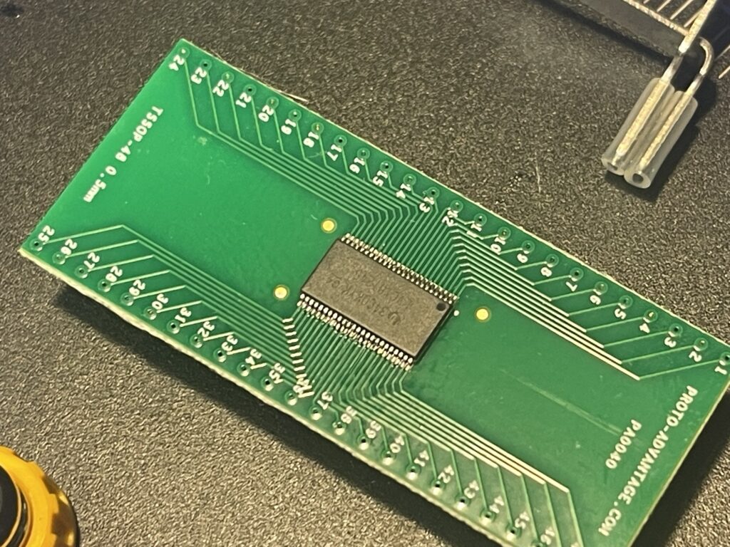
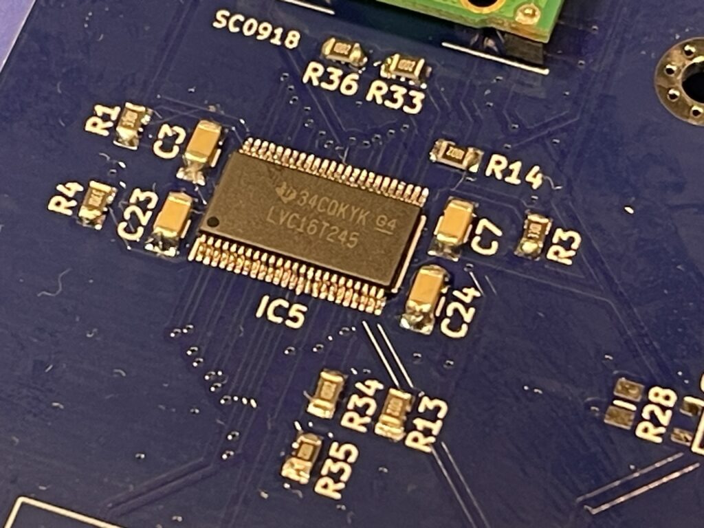
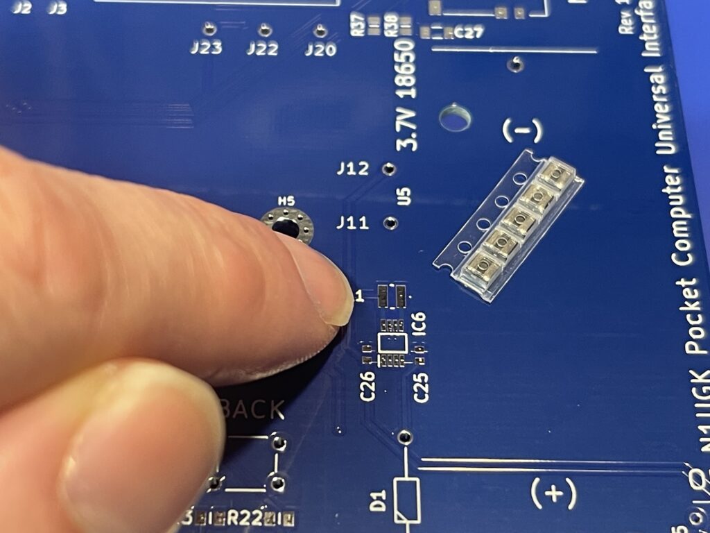
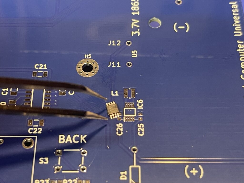
Surface Mount Components
As mentioned earlier, the choice of using surface mount components was practicality. Most often, the component I wanted to use was available only in SMT. Further, if I chose a through-hole component, often times it was being phased out. The down side to SMT is that it is more difficult to solder them onto a PCB by hand. It is not however impossible.
Another downside to SMT is breadboarding is more costly. In a DIP style package, you can press a component into a breadboard and test an idea. With SMT, more often than not, some creative solutions are needed for breadboarding. For example, on the bus interface IC I chose, it is available only in SMT, and I ended up using an SMT to DIP PCB. I soldered the component to this PCB then used the pins on the other side for a breadboard and direct test clip leads.
Of course the breadboarding was quite easy compared to soldering the component itself onto the PCB. A fine soldering tip with the correct heat setting, the right flux, magnifier glasses, and a steady hand proved to be successful.
In some cases, creative methods are needed for breadboarding. I ended up using BS138 FETs for voltage level shifting and these were readily available as SMT. I ended up soldering small bodge wires to each pin and inserting those into the breadboard.
Very rarely was an SMT part overly difficult to solder to the PCB. The exception was an inductor needed on the power supply circuit which had two pads underneath the component.
Software Design
The software for the PCUI utilizes the C SDK for the Pico, as opposed to the Python SDK. I had no desire to use Python and I have decades of experience in C and similar languages.
Since I am using an I2C bus for many ICs and the OLED, the challenge in the software design is in the interfacing with the pocket computers themselves, not the basics like MicroSD card usage, OLED, Parallel, Serial, memory management, and user interfaces.
I found it extremely difficult if not impossible to successfully interface using the GPIO method with a single interrupt. My timing was off, there were missed pin changes, complex and confusing logic to try to implement workarounds for the single interrupt issue using GPIO methods.
I ended up taking advantage of the Pico’s state machine feature, or PIO. With the Pico, you can have up to 8 state machines running independently from the two cores. PIO has an assembly language and each state machine program can be up to 32 lines of code.
As a POC, I implemented the TI graph link protocol for sending and receiving in PIO assembly. I have one state machine handling receiving and another handling transmitting.
Each state machine can push or pop to and from a FIFO via DMA and can generate interrupts for the cores for processing.
The PIO state machine instructions operate in a single clock cycle, which is extremely fast. For example, the Pico is fast enough to directly generate VGA signals directly from PIO and leave the two cores available to process information.
The PIO state machines support a clock divider to step down the processing speed or instruction cycle to best match the needs of what it is connected to.
The PCUI software will utilize the OLED and four soft keys for a user interface for selecting various modes and options for interfacing with various pocket computer models and printers.
It will use a MicroSD card to store data, screen captures, programs and more.
Useful Methods and Process
Some of the most useful process and methods are what makes projects like this easier to succeed. First, I found that it is crucial to label the PCB with a board revision and save a corresponding PDF of the schematic with the same revision labelling. Sometimes you might want to test something with a spare or leftover board, and revision is key. Then you may want to consult the schematic for that revision. If you do not save copies of previous revisions, you are left with more work tracking down a problem.
Not to mention, if any PCB revision makes its way out into the world, labelling of revisions and having the corresponding schematic for that revision could help others troubleshoot or repair.
Another crucial step in the design process is breadboarding and prototyping. Each circuit should be tested on a breadboard and its integration with the rest of the circuit tested as well. Otherwise, you will find yourself ordering more revisions of your PCB than you should be. Not only is this a waste of money, it adds delay to your timeline.
Component choice is also important, not only for cost, but for longevity. For example, choosing a battery that is commonly used is helpful for projects sold as a kit for others to build. If a battery is chosen which becomes discontinued or difficult to obtain, the kit is more difficult to assemble.
Similarly, finding a microcontroller that will likely be around for awhile, and one which will likely see a compatible successor is key. Not only will it be helpful to have something commonly used for advice and help, your software will not need a complete rewrite for another microcontroller when your existing design choice is obsolete.
Another example is the choice of OLED screen. I chose one which I can easily acquire for around $1 each and is commonly used. Lastly, if a project requires connectors, a choice of a common inexpensive connector style is key. This ensures product longevity and avoids the infamous proprietary connector issue we most often see with pocket computers.
Finally, I found it most useful to track a bill of materials for each revision. This way I can quickly and easily reorder components either all at once in various quantities and also be able to share the component list with others who might want to built their own as a kit.
This tracking can be done in a spreadsheet or in software. KiCad and Mouser for example can do this for me.
Final Thoughts
This is my biggest project of its kind that I started a few months ago now. It will likely continue to evolve until a useful version is ready for sharing.
Since the interest in something like this is small, production of this device pre-assembled would be cost prohibitive. I plan to offer these for sale fully assembled.
The software will be pre-flashed on the Pico, and is easily updatable by downloading the latest image and dropping it into the folder which appears when it is plugged into a Mac or PC.
I plan to publish more posts and videos as the PCUI is closer to production ready. If you are reading this and have interest in this kit, please reach out to me via my contact page on this blog.
Behind the Scenes
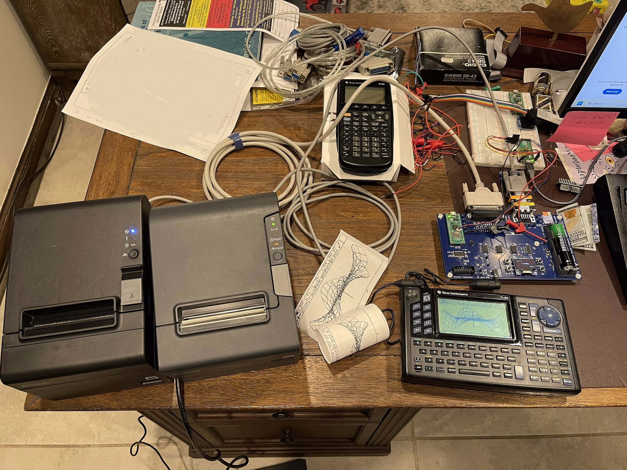
Below are some photos I have taken along the way as I finished some of the hardware and software components for the project.
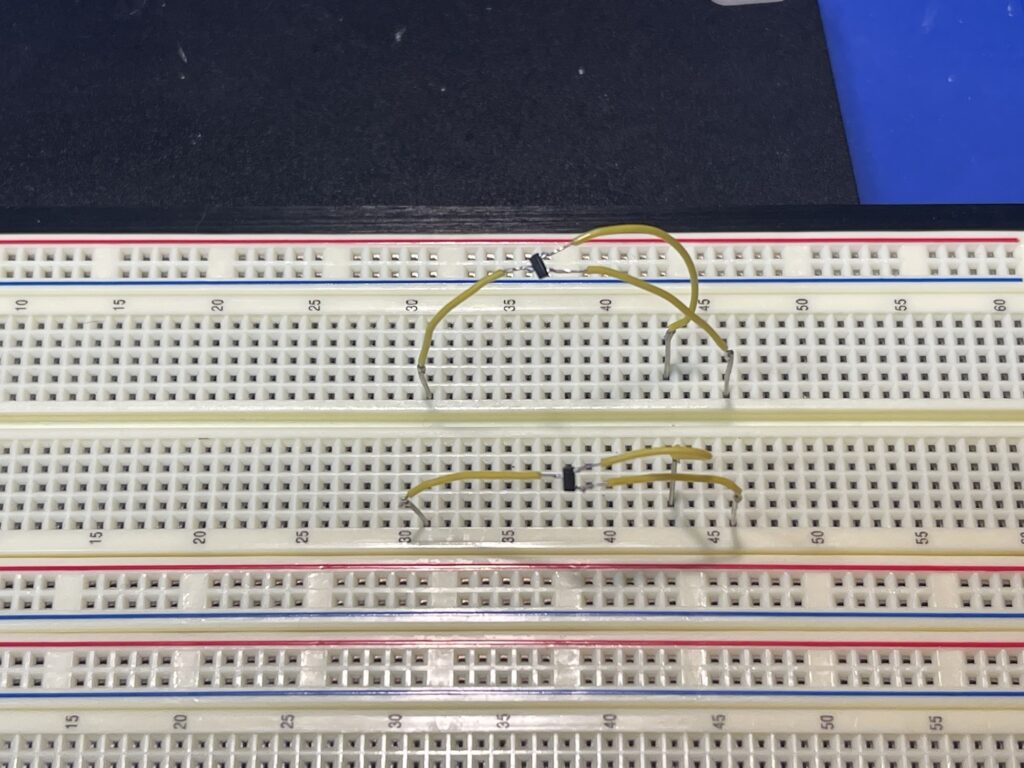
There was quite a bit of breadboarding of SMT components and testing level shifting, lots of thermal paper used for failed attempts at printing and scaling of screen captures.
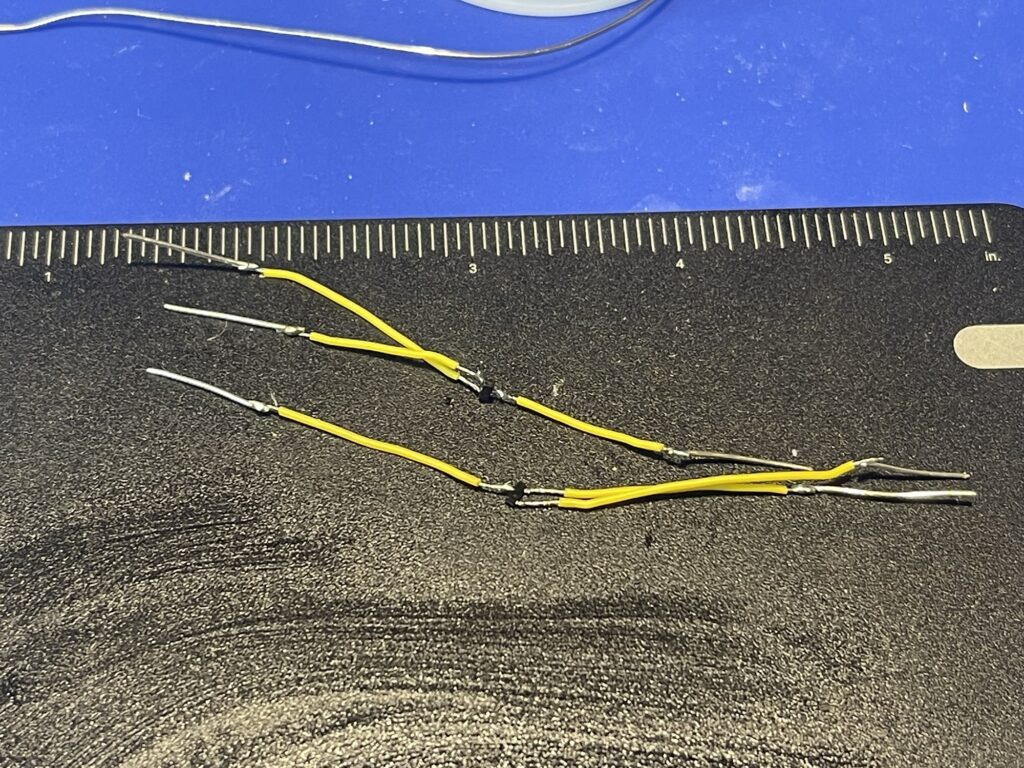
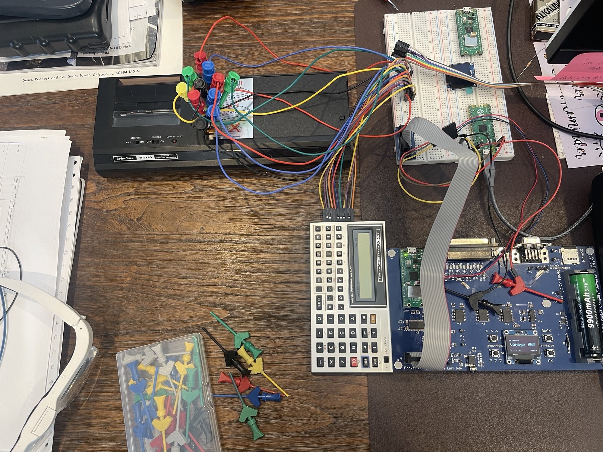
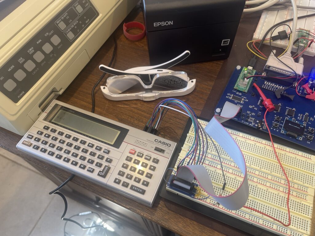
Before making the first PCB, the amount of wires needed to sniff the bus on a PB-410 as an example was unwieldy.
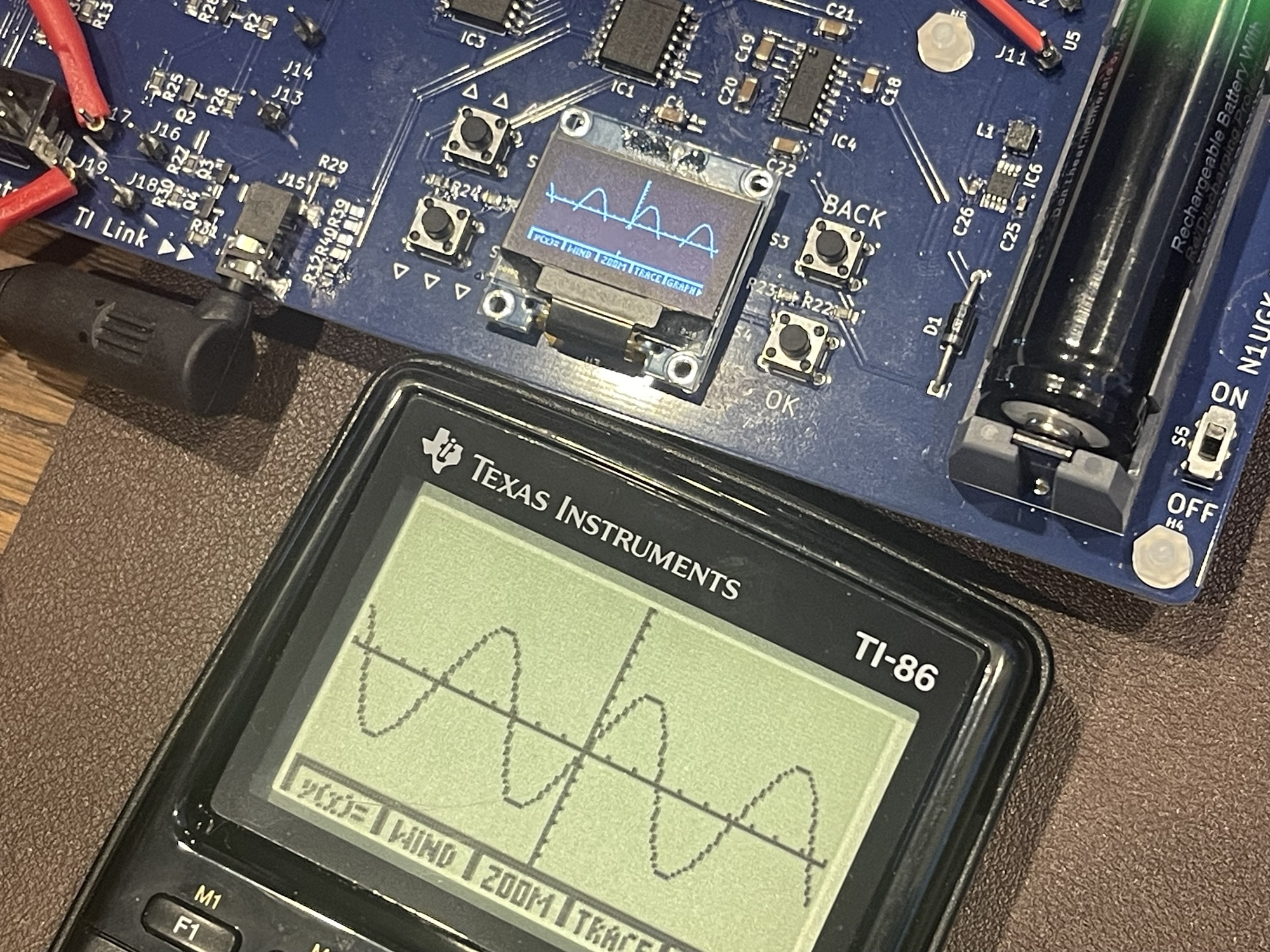
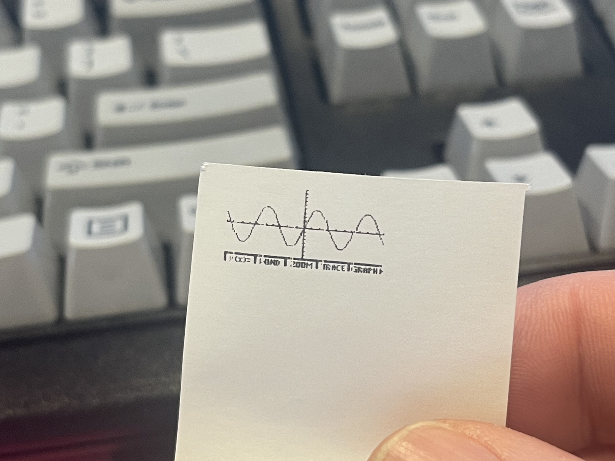
Since the TI graphing calculators support screen captures, this was the primary feature built out first, screen capture to print out on an attached serial or parallel printer. Scaling was also implemented to take advantage of the available paper sizes.
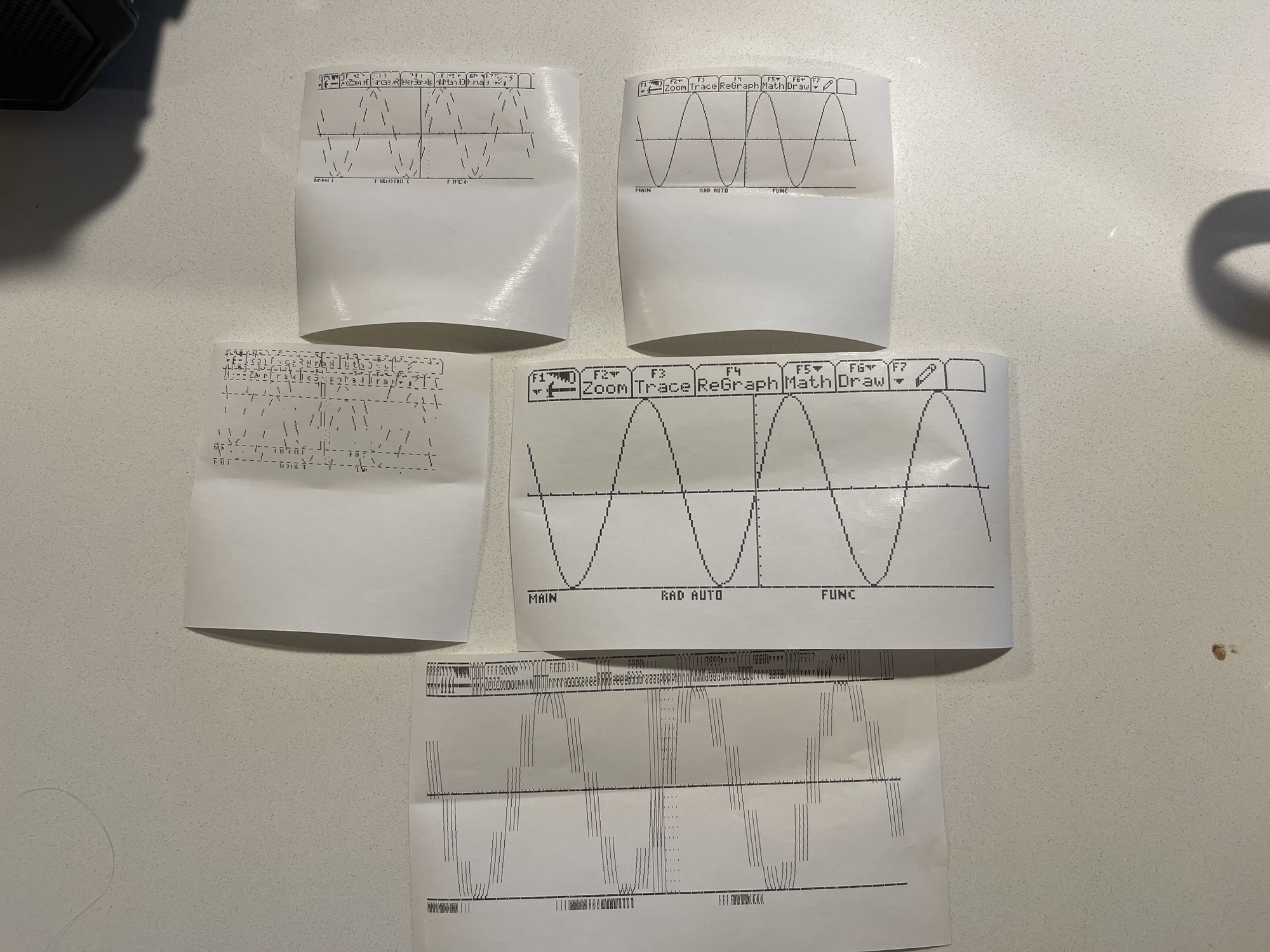
Epson ESC/POS provides for graphics or bitmap printing, and some printers need workarounds or specific methods to print a bitmap image without any line gaps.
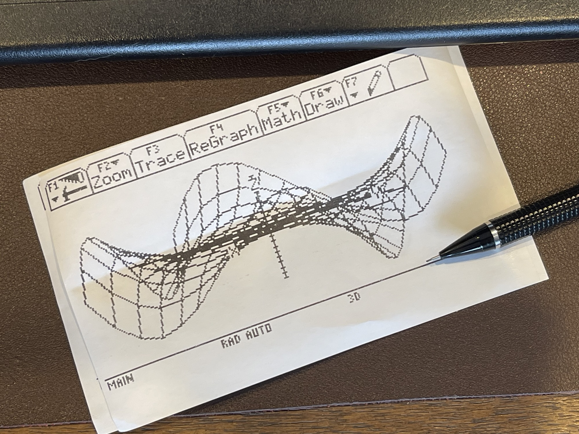
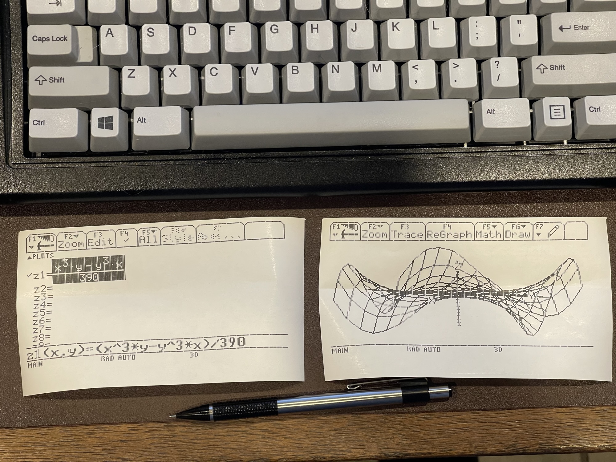
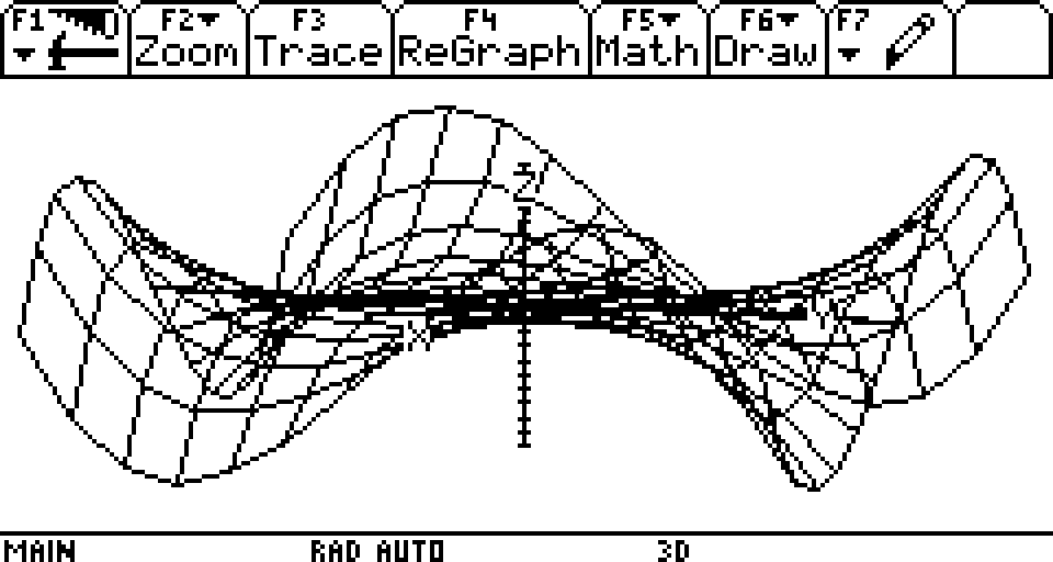
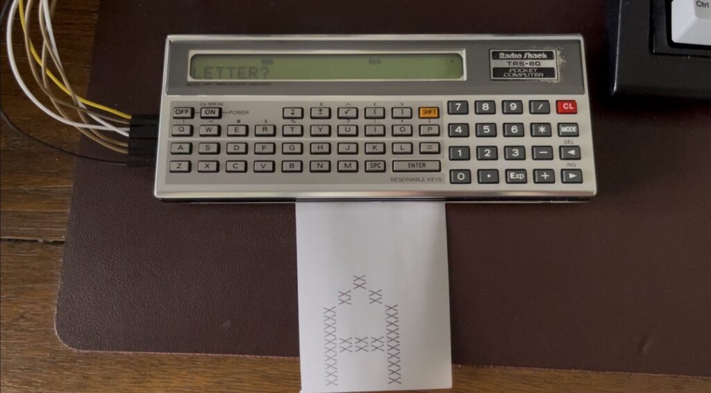
Since printing a screen shot might not be the only useful feature, the PCUI generates a PNG image of each screen capture and writes them to the MicroSD card. Below is an example of a PNG screen capture from a TI-92 displaying a 3D graph:
Plugging the PCUI into a PC or Mac can be done using the micro USB port. The PCUI appears as a drive, exposing the MicroSD card to the PC or Mac. This allows for easy copying of the PNG captures for using them in manuals, publications, or elsewhere.
Finally, the PCUI has a TI Graph Link “passthrough” mode. This mode translates between the graph link port and the RS-232 port. This allows the PCUI to become a “gray link” cable. The gray link cable was a TI produced cable which connected a calculator to a PC via the serial port. This allows the PCUI to work with TiLP, without the need for a TI interface cable.
Sharp PC-1246 / Tandy PC-8 Progress
The Sharp and Casio (and RadioShack / Tandy) pocket computers interface with cassette storage by using audio frequency shift keying (AFSK). This means that I cannot simply receive serial data from the pocket computers when they save to tape, nor can I send serial data to them when loading from tape.
AFSK generated by an output pin at TTL level can be seen visually as a square wave (zeros and ones) at two frequencies. I took the capture below from my $8 USB based logic probe:
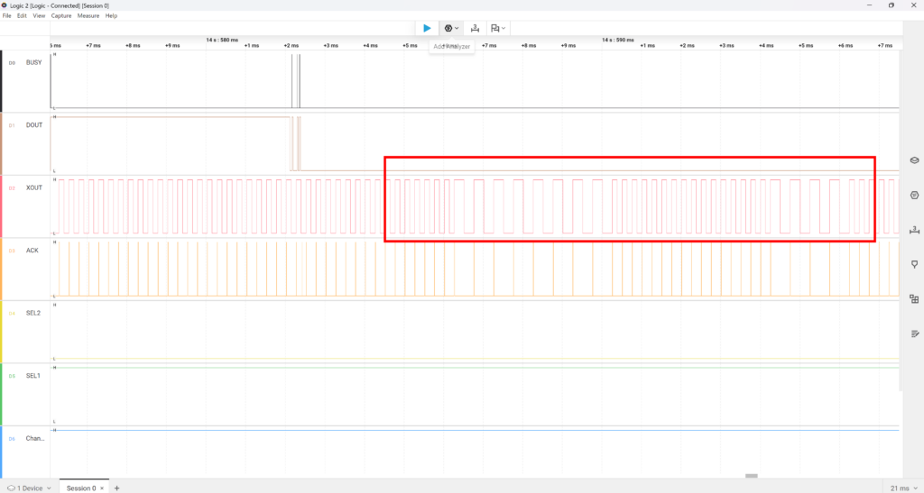
In the image above, there are clearly two different frequencies generated by the pocket computer. There is a 2000 Hz and 4000 Hz tone pair. The PCUI can detect these two frequencies and translate them into the bitstream that the pocket computer is sending. The PCUI can also perform the inverse – generate an AFSK output for loading programs into the pocket computer.
The PCUI uses these methods to load and save programs to and from the micro SD card. This emulates an attached cassette recorder, which allows hobbyists who do not have the cassette interface to store and load programs.
I am impressed by these Casio and Sharp pocket computers in how they were able to decode AFSK streams from cassette tape, with such little memory. The sync, checksum, and robustness of the protocol is impressive.
Building an encoder and decoder for the PC-1246 (Tandy PC-8) was not a simple task at all. I needed to use a PIO state machine for the encoder and another for the decoder.
Now the PCUI can save programs and data from the PC-1246 to the micro SD card, as well as send programs and data stored on the micro SD card. It performs these tasks with a direct connection to the pocket computer. In theory, this would also work with other Sharp models that have the 11-pin connector, such as the PC-3, the PC-8, other variants of the PC-12xx, and perhaps others.
Printer Emulation
I was able to get the PCUI to emulate an attached printer, such as the Sharp CE-126P thermal printer or the TRS-80 PC-3/PC-8 printer. The PCUI accepts and responds to the signaling by the PC-8/PC-1246 to receive the bytes sent and then direct them to either the parallel or RS-232 port on the PCUI.
This provides support for standard line printers to be used with the PC-8 (and similar models).
At this point, the PCUI provides a complete printer and cassette interface for this and similar models with the 11-pin connector.
It is interesting to see that the PC-8 (and similar models) send ASCII character codes out when printing, but their internal code page is not ASCII. For example, the tokenization of BASIC programs and any literal strings are not ASCII, but when characters are sent to the printer, they are. This means that these models need to translate their own code page to ASCII when printing.
This also indicates that the firmware for the printer (the actual printer controller, not the interfacing CPU) was built to work with ASCII. This makes sense, as these thermal printer mechanisms needed to work with a standard and were likely not manufactured for Sharp (nor Casio) but rather an off the shelf part used in other devices at the time.
Casio PB-100, FX-7xx,FX-8xx / Tandy PC-4, PC-5, PC-6 Progress
After finishing up the Sharp PC-1246 support, I moved on to the other large batch of pocket computers I own, the Casio PB-1xx, FX-7xx, FX-8xx and Tandy PC-4, PC-5, PC-6 models. This was a challenge in a different way, as the way the printers work with these models is really quite a hack.
These models do not put data out on the bus when printing – they require the printer to go into a specific area in memory in the pocket computer and fetch the bytes to be printed. The interfacing with these models for the printer support is more of a “bus” interface than a serial-like interface like with the Sharp.
Saving and loading of programs, variables, and memo content was much easier than the Sharp interface since these Casio models use a pin on the data bus and handshaking for the tape interface as opposed to AFSK on pins in the Sharp.
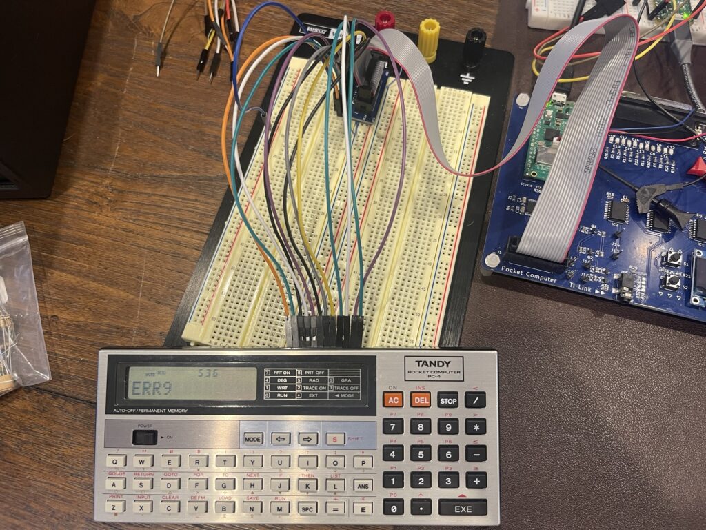
The PB-100 (Tandy PC-4) ended up testing my limits in patience and capability. I performed all of my development using the “B” version of this model which for the PC-4 was labelled as “Tandy” as opposed to “TRS-80” PC-4.
The printer mode did not work at all with the PCUI on the earlier model. I ended up having to make a hardware change on the interface pack for these models, purchase a better logic analyzer, and completely redoing the cassette protocol emulation as I began using it and found a few significant bugs.
I ended up sniffing the bus again, this time with a much better logic analyzer and a test harness. The results proved successful, after weeks of dead end attempts at guessing.
Casio FX-702P Progress
Next up for prototyping was the Casio FX-702P series of pocket computers. Hopefully the same 7 pin connectors found on the FX-602P and the FX-502P will provide printer support for those as well.
The FX-702P uses signaling at CMOS levels, which is different from the other models I previously added support for. As a result, I needed a board revision to add a connector for CMOS level devices.
I was looking forward the most to this series working with the PCUI because the printer for this series is the FP-10 spark printer with unobtainable aluminum coated printer paper. Having this work with a modern thermal printer would be the only viable way to print these days with this series.
After much trial and error, I was finally able to get the printer and cassette interfacing for the PCUI for this model. In theory, this should also work with the FX-602P, the FX-502P, or any other model with the 7 pin connector.
Casio PB-700 / PB-770 Progress
The Casio PB-700 is yet another series of models which vary slightly from the PB-100 series. The printer support is more direct, meaning the PCUI does not need to be a bus master and pull nibbles out of specific memory locations in the pocket computer. Instead, the nibbles are placed on the bus by the pocket computer, allowing for a simpler implementation. In fact, the FA-4 is a discrete component implementation of a parallel port adapter basically using flip-flops, gates, level shifters, and inverters.
Another item of note is that the printer output is mostly ASCII, with some custom characters in the extended regions. What is most interesting is Casio released only the FA-4 for “standard” Centronics printer connections (try to find one of those these days), and the FA-10, which has the cassette interface and a four color plotter (like the PC-2 but bigger).
Adding standard printer support to these models was exciting because I can use any standard parallel or serial printer such as an ESC/POS thermal printer or a dot matrix printer. I am no longer limited to the four color plotter, which uses pens and might have cracked pinion gears and anti-backlash gears.
Tape support is similar to the PB-100 except there is no memo feature and there are more options for transfer such as ASCII. This allows saving to a TXT file in the PCUI and then you can directly edit on the micro SD card, then send back to the PB-700. Or, you can copy programs from book(s) and drop the text files on the micro SD card and send them to the PB-700.
PCUI Prototype with the Casio PB-700
Plotter Emulation
The PB-700 and PB-770 had the FA-10 four color plotter, which I restored one and created a maze program for. Interestingly, these plotters not only support drawing shapes, lines, etc, but they also can draw “text”. It is not the most efficient type of printer for printing text, but it does a good job.
Using a more modern thermal printer such as an Epson POS printer is a nice upgrade, with inexpensive paper and no pens to refill or seek out. However, this provides only a text based replacement – any programs which printed using plotter features would not work on the ESC/POS printers, as they do not support the same line and shape commands.
I added a feature on the PCUI to accept the FA-10 plotter commands and render the result to a canvas in memory in the PCUI. The PCUI then listens for the escape back to “character mode” from the PB-700, then saves the canvas to PNG, then prints it as a bitmap to the ESC/POS printer.
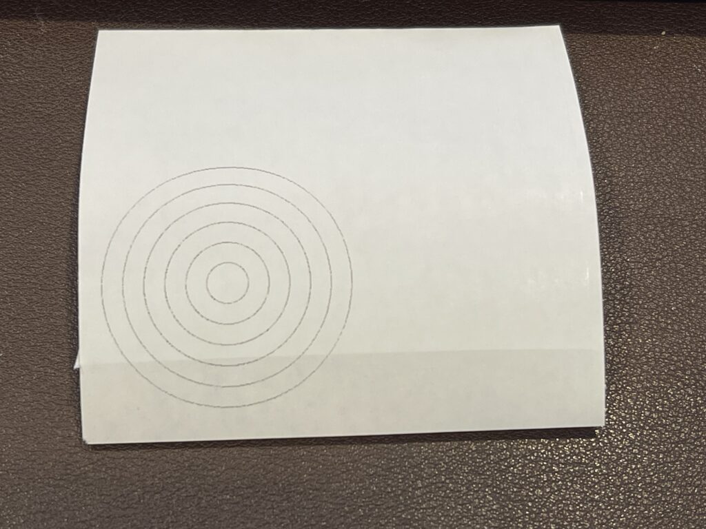
Below is an example from the FA-10 manual to plot a series of concentric circles:
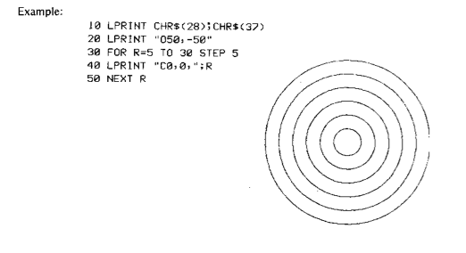
Of course, given the example above, I added a line 60, which returns to character mode. This is the PCUI trigger to save and print the canvas. As a test, I entered the same program as in the example, and the result is below:
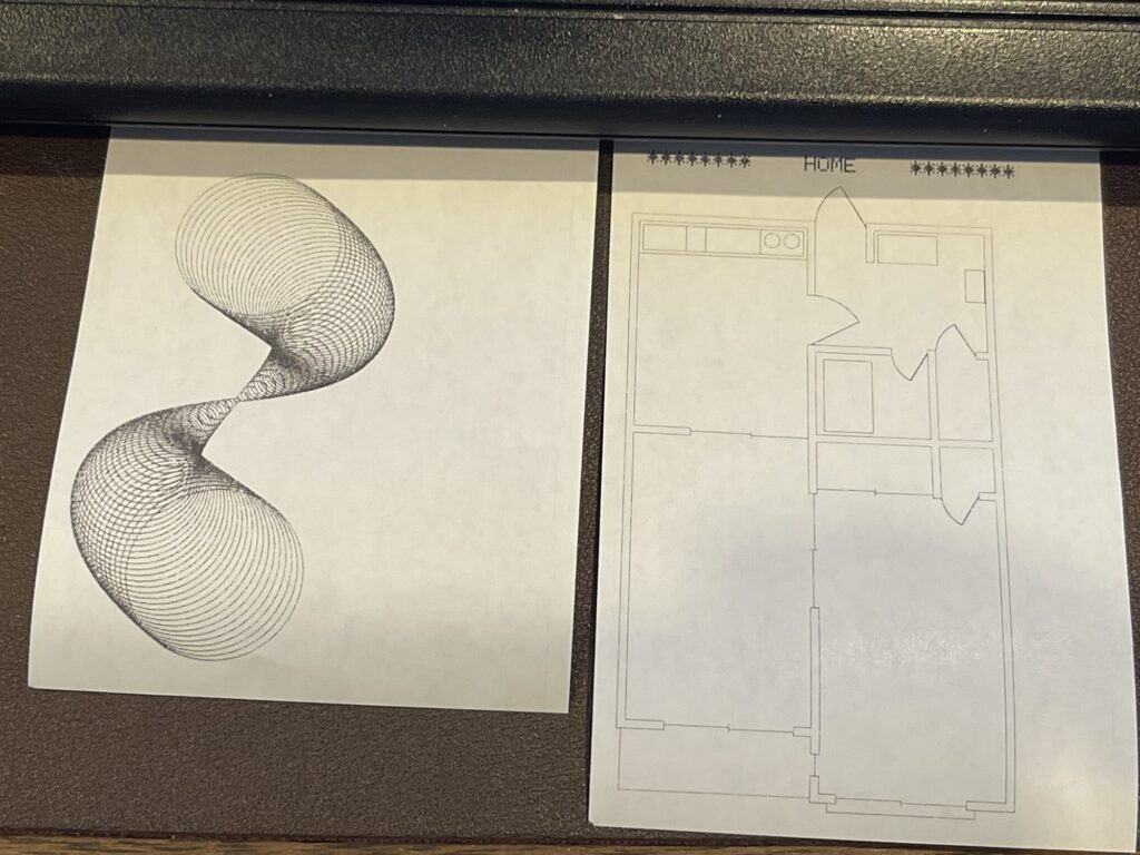
For the PB-1000 and FX-880P, I modified a version of the “globe” program and plotted it on the larger full size FP-100 plotter. I modified the program for the PB-700 / PB-770 and ran the program with the plotter emulation:
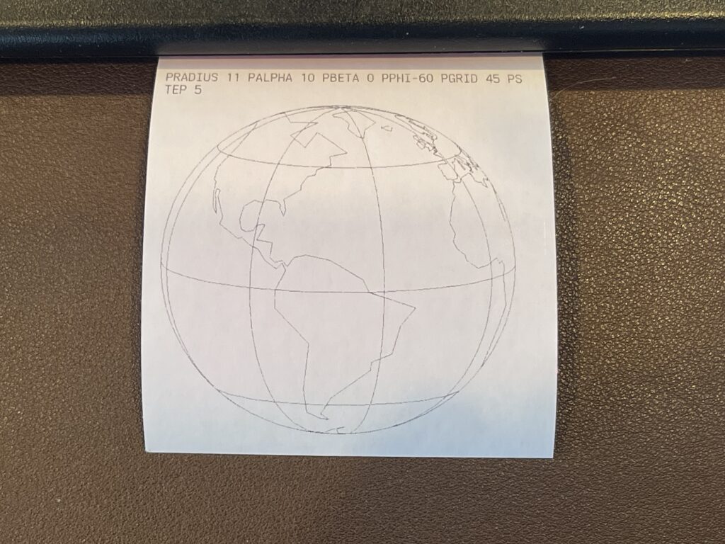
The plotter emulation feature in the PCUI allows for programs which utilize the plotter to be used with modern printers. Many sample programs in the owners manuals include plots, and those will now run without losing the plotting functionality.
In addition to ESC/POS, IBM ProPrinter support was added to the PCUI, so any dot matrix printer with ProPrinter support can be used in a similar fashion.
In addition to keeping plotting functionality intact on the PB-700 and PB-770, the PCUI can accept these commands from any pocket computer, even if that model did not offer a plotter. That brings plotter features to any pocket computer connected to the PCUI.
Sharp PC-1401 Support
The newer Sharp models with the 11-pin connector that also support the CE-126 printer use a variation on the protocol compared to the older models such as the PC-1246.
The CE-126P, according to the service manual, supports a dual interface, one for the older models and another for the newer models (which do not use the 2 select lines).
Adding support for the PC-1401 and other newer models was far easier since I could build off the existing PC-1246 support.
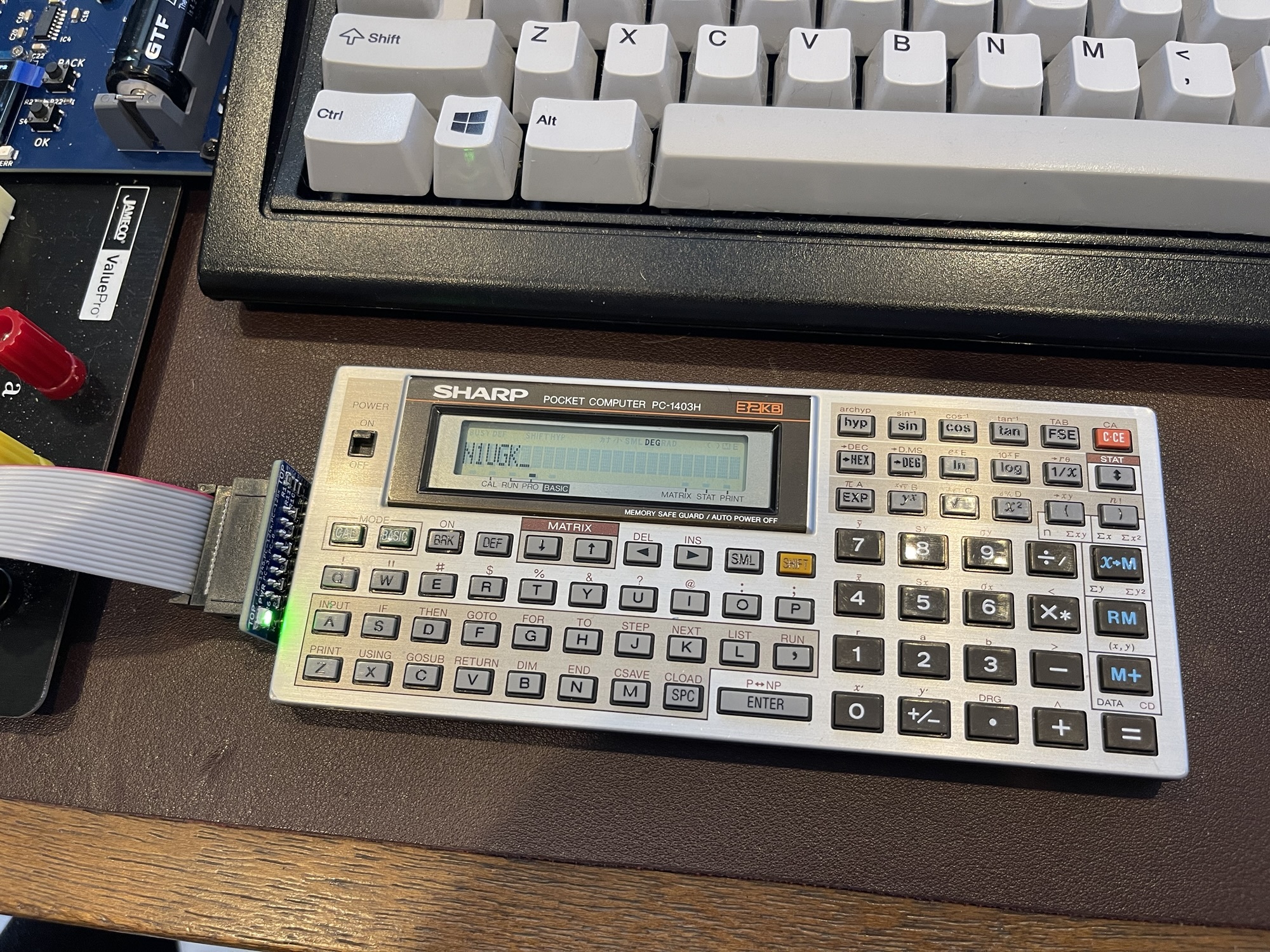
PCUI Prototype with the Sharp PC-1403H
When adding support for this series of pocket computers from Sharp, I added a new PCUI feature which will convert a BASIC file in ASCII format (on the SD card) to a tokenized version on the fly. This provides a convenience to allow editing or copy & paste from a source on your PC or Mac and load it directly into the pocket computer using the binary loading/cassette interface.
Sharp PC-1211 / Radio Shack TRS-80 Pocket Computer PC-1
Sharp’s first BASIC programmable calculator series included the PC-1210 and the PC-1211. The TRS-80 Pocket Computer (PC-1) was the Sharp PC-1211, the first pocket computer in Radio Shack’s lineup. This model uses a 9-pin expansion port, unlike the 11-pin port found on future models. This 9-pin port is completely different in terms of interfacing compared to the later models.
The cassette interfacing is different in that it is asymmetric – in one direction the PC-1 uses AFSK, in the other direction it is a serial-like connection.
The printer interface is different as well, quite simple, compared to the newer Sharp printer interfacing. It uses the same serial line as the cassette serial line, and a similar framing.
Getting this model working with the PCUI was exciting because this finishes off the entire line of pocket computers radio shack sold, minus the PC-2 (which already has modern options for connectivity) and the PC-7 which does not have an expansion port.
Latest Board Revision – Release Candidate
The latest board revision has been tested and working as expected.
This latest version adds the CMOS level interface packs (for the FX-502/602/702). It also adds LED status indicators. There is also an RS-232 jumper pad for switching RX/TX lines avoiding the need for null modem adapters when switching connections between a printer and a computer for example.
This is likely the first version that I will offer for sale as a completely assembled package.
Wi-Fi Connectivity and Program Sharing
Wi-Fi connectivity is available for accessing files on the PCUI’s micro SD card, viewing the screen and controlling the PCUI. From the web interface you can download files, edit files, rename and delete files.
With the web interface, you can edit a saved BASIC program stored on the PCUI using a text box, then save it. The PCUI can then tokenize it on the fly when sending to the pocket computer, which makes program edits much quicker and easier.
It would be possible in the future for the PCUI to connect to a repository “online” and display programs available for download. Perhaps this would be useful for sharing programs.
The PCUI, when attached to a TI graphing calculator, offers a web based view of the screen, which updates automatically:
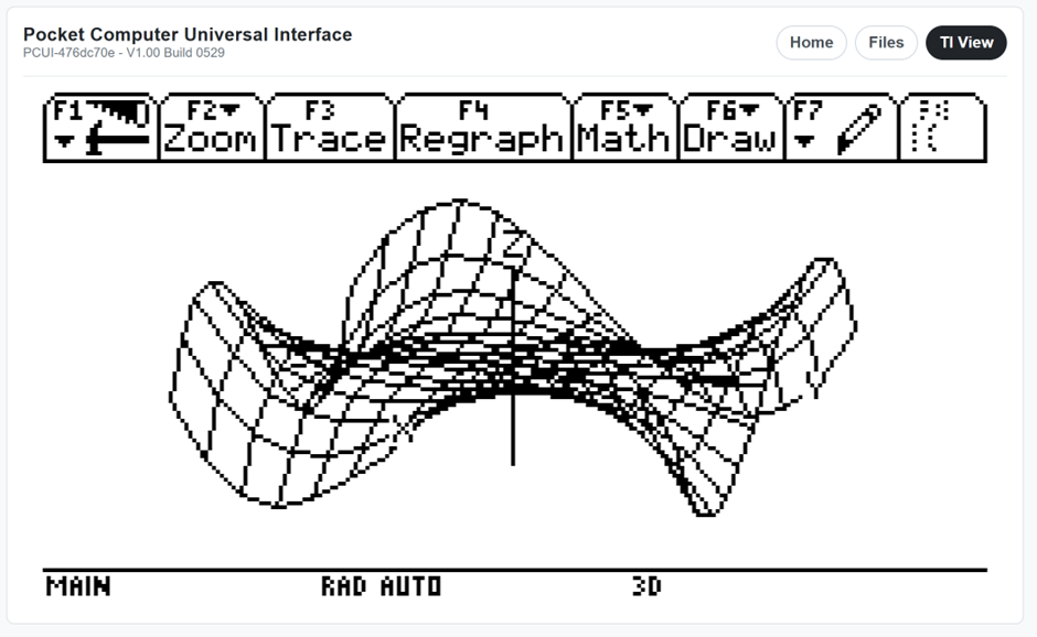
In addition to the screen view, the PCUI accepts keyboard input on the page, allowing you to control the attached TI-92, TI-92+, and Voyage 200.
hi N1UGK, I finally got to read this article and I think this is a great project to implement, we all have a plethora of sharp, Tandy & Casio Pocket computers with their own proprietary interfaces, so making an all in one solution, is cool. I started building an interface for the sharp PC-1460, my pocket computer from engineering at Umi in the 1980s. A guy who goes by the handle Codaris has created an interface and you need an Arduino Nano, and a few pulldown resistors to make it possible to upload and backup programs. I can’t wait to finish it, and try programming it again. I would still like to get one when its ready and look forward to supporting it, with any testing or whatever. Rgs Shawn
Hi Shawn, I’m curious to see the interface you’re building – perhaps you can share the info about it on my contact page. I’m trying to collect as much information from others that created interfaces, and you would be surprised at the level of hackery (casio for example) for the method of printing to an attached printer. Anyhow, once I get a bit further in design validation, I’ll add your info to my list of those who I can send some kits to for testing.